Method of preparing nano-level metal grid transparent conductive film

A technology of transparent conductive film and metal grid, which is applied in the direction of nanotechnology, circuits, electrical components, etc., can solve the problems of passing through, not solving nanoscale graphics, and inability to perform photolithography, etc., and achieve the effect of simple process

Active Publication Date: 2015-10-07
WUXI MESH TECH CO LTD
View PDF8 Cites 9 Cited by
  • Summary
  • Abstract
  • Description
  • Claims
  • Application Information

AI Technical Summary

Problems solved by technology

Although this invention overcomes the problem of the complexity of the nanometer-scale pattern manufacturing process of the existing mask plate, at the same time, due to the limitation of the diffraction limit, it cannot be passed through by general wavelength or long wavelength light, and cannot be used for photolithography.
However, the preparation of the mask plate described in the invention needs to form a metal thin layer with a nanometer-scale fine pattern structure on the substrate surface, and the process of forming a metal thin layer with a nanometer-scale fine pattern structure on the substrate surface still needs Obtained by using a mask with nanometer-scale patterns, which fundamentally does not solve the difficulty of making nanoscale patterns on large-scale masks

Method used


Image

  • Method of preparing nano-level metal grid transparent conductive film
  • Method of preparing nano-level metal grid transparent conductive film
  • Method of preparing nano-level metal grid transparent conductive film

Examples


Embodiment 1

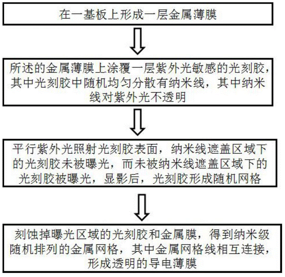
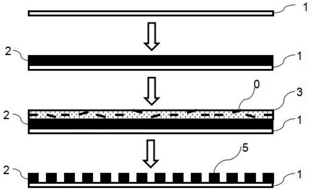
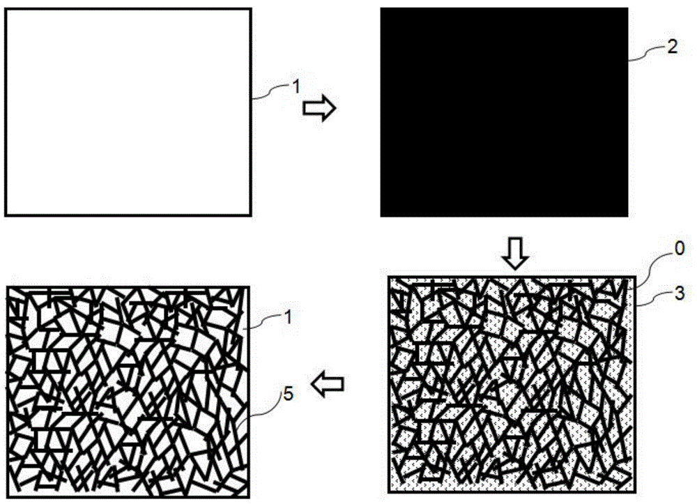
[0035] A method for preparing nanoscale metal grid transparent conductive film, such as figure 1 , figure 2 , image 3 , Figure 4 shown, including the following steps:

[0036] 1) forming a layer of metal thin film 2 on a substrate 1;

[0037] 2) Coating a layer of UV-sensitive photoresist 3 on the metal film 2, wherein the photoresist 3 is randomly and uniformly dispersed with nanowires 0, wherein the nanowires 0 are opaque to ultraviolet light;

[0038] 3) Parallel ultraviolet light irradiates the surface of the photoresist 3, the photoresist 3 under the area covered by the nanowire 0 is not exposed, and the photoresist 3 under the area not covered by the nanowire 0 is exposed, after development, the photoresist 3 form a random grid;

[0039] 4) Etching away the photoresist and the metal film in the exposed area to obtain a metal grid randomly arranged at the nanoscale, wherein the metal grid lines 5 are connected to each other to form a transparent conductive film. ...

Embodiment 2

[0044] A method for preparing nanoscale metal grid transparent conductive film, such as Figure 5 , Figure 6 , Figure 7 , Figure 8 shown, including the following steps:

[0045] 1) forming a layer of metal thin film 2 on a substrate 1;

[0046] 2) Coating a layer of UV-sensitive photoresist 3 on the metal film 2;

[0047]3) Apply a layer of high light-transmitting resin 4 on the photoresist 3, wherein the high light-transmitting resin 4 is randomly and uniformly dispersed with nanowires 0, wherein the nanowires 0 are opaque to ultraviolet light;

[0048] 4) Parallel ultraviolet light is irradiated on the surface of the high light-transmitting resin 4, and the photoresist 3 under the area covered by the nanowire 0 is not exposed, while the photoresist 3 under the area not covered by the nanowire 0 is exposed. Glue 3 forms a random grid;

[0049] 5) Removing the high light-transmitting resin 4, etching away the photoresist 3 and the metal film 2 in the exposed area, and...


PUM

PropertyMeasurementUnit
thicknessaaaaaaaaaa
diameteraaaaaaaaaa

Abstract

The invention discloses a method of preparing a nano-level metal grid transparent conductive film. The method includes the following steps: firstly, forming a metal film on a substrate; secondly, coating the metal film with a photoresist sensitive toultraviolet light, wherein nano wires are randomly and evenly dispersed in the photoresist, and the nano wires are opaque to ultraviolet light; thirdly, irradiating the surface of the photoresist with parallel ultraviolet light, wherein the photoresist covered by the nano wires are not exposed, the photoresist not covered by the nano wires are exposed, and the photoresist forms random grids after development; and fourthly, etching the photoresist and the metal film in the exposed area and obtaining nano-level randomly-arranged metal grids, wherein the metal grids are connected to each other to form a transparent conductive film. The nano wires are utilized to serve as masks, difficulties in preparing nano-level patterns on a large-scale mask slice are overcome, graphical effects of nano-level random grids are achieved, processes are simple, and roll-to-roll large-area batch production is facilitated.

Description

technical field [0001] The invention relates to the technical field of nanoscale photolithography patterning, in particular to a method for preparing a nanoscale metal grid transparent conductive film. Background technique [0002] With the rapid development and maturity of electronic technology, and people's extreme pursuit of lighter and thinner electronic equipment, there is an urgent need for micromachining technology to produce high-speed and high-frequency nanoscale devices, and microstructure patterning is an important aspect of micromachining. A very important one in technology is also getting more and more attention. In the prior art, microstructure patterning technologies mainly include phase difference enhanced imaging technology, imprinting technology and photolithography technology, among which photolithography technology is the most common metal thin film patterning processing technology. Microstructure lithography patterned metal thin film mainly adopts the m...

Claims


Application Information

Patent Timeline
Patent Type & Authority Applications(China)
IPC IPC(8): H01B13/00B82Y40/00
Inventor 王振中
Owner WUXI MESH TECH CO LTD
Why Eureka
Try Eureka