Transparent conducting thin film and manufacturing method thereof
A technology of transparent conductive film and conductive film, applied in the direction of ion implantation plating, coating, metal material coating process, etc., can solve the change and improvement of conductivity and light transmittance limited, cannot be flexibly adjusted, ITO price Overexpensive and other issues, to achieve excellent quality, reduce complexity and environmental requirements, and improve optical performance
- Summary
- Abstract
- Description
- Claims
- Application Information
AI Technical Summary
Problems solved by technology
Method used
Image
Examples
Embodiment 1
[0044] Step 1, using H 2 -Ar mixed gas plasma method to treat the substrate surface and activate the surface;
[0045] Step 2, depositing a layer of prefabricated titanium nano-metal layer on the flexible substrate PET, the conditions are as follows:
[0046]
[0047] Step 3, use sputtering equipment to sputter doped zinc oxide film on the prefabricated layer, and the sputtering conditions are as follows:
[0048]
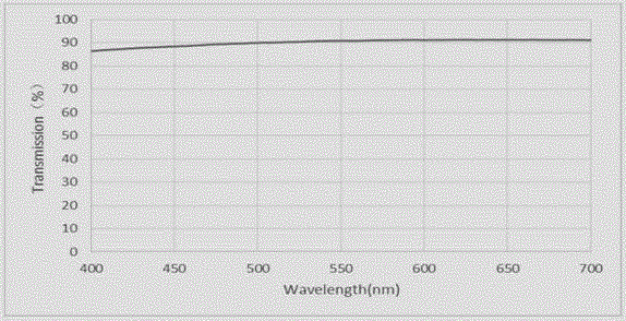
[0049] The average light transmittance in the visible light region is >70%, and the resistivity is -3 ohm cm
[0050]Step 4, sputtering a silver film on the existing doped zinc oxide film with a sputtering device, the sputtering conditions are as follows:
[0051]
[0052]
[0053] Step 5, using sputtering equipment to sputter doped zinc oxide film on the existing silver film, the sputtering conditions are as follows:
[0054]
[0055] The average light transmittance in the visible light region is >70%, and the resistivity is -3 ohm cm;
[0056] ...
Embodiment 2
[0058] Step 1, use a sputtering device to sputter a doped zinc oxide film on the PET that has undergone plasma surface treatment, and the sputtering conditions are as follows:
[0059]
[0060] The average light transmittance in the visible light region is >70%, and the resistivity is -3 ohm cm;
[0061] Step 2, sputtering a silver film on the existing doped zinc oxide film with a sputtering device, the sputtering conditions are as follows:
[0062]
[0063] Step 3, use sputtering equipment to sputter doped indium oxide film on the existing silver film, the sputtering conditions are as follows:
[0064]
[0065] The average light transmittance in the visible light region is >70%, and the resistivity is -3 ohm cm;
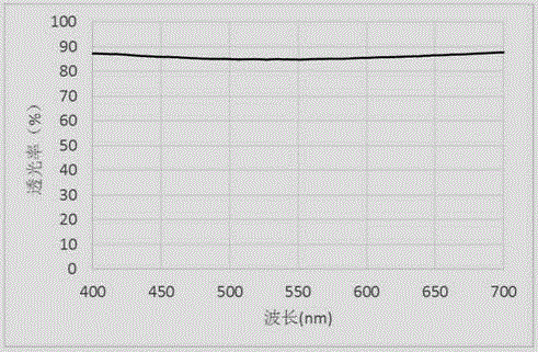
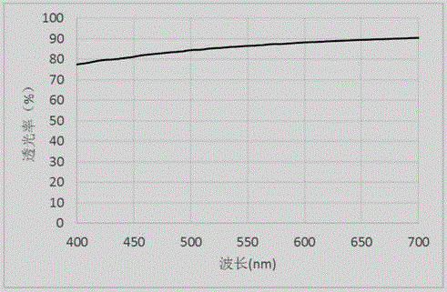
[0066] Result: light transmittance 84%, resistivity 2×10 -4 Ω. cm.
Embodiment 3
[0068] Step 1. Use a sputtering device to sputter a doped zinc oxide film on ultra-clear glass through plasma surface treatment, and the sputtering conditions are as follows:
[0069]
[0070] Step 2. sputter silver film on existing doped zinc oxide film surface with sputtering equipment, sputtering condition is as follows:
[0071]
[0072] Step 3. sputtering doped indium oxide film on the silver film with sputtering equipment, the sputtering conditions are as follows:
[0073]
[0074] The average light transmittance in the visible light region is >70%, and the resistivity is -3 ohm cm;
[0075] Result: light transmittance 85%, resistivity 2×10 -4 Ω. cm.
PUM
| Property | Measurement | Unit |
|---|---|---|
| thickness | aaaaa | aaaaa |
| thickness | aaaaa | aaaaa |
| thickness | aaaaa | aaaaa |
Abstract
Description
Claims
Application Information


