Digital photoelectric magnification device

A digital, digital value technology, applied in the field of photoelectric detection devices, can solve the problem of not being called an image sensor, not given, etc.

Active Publication Date: 2015-11-11
WUHAN JOINBON TECH CO LTD
View PDF4 Cites 14 Cited by
  • Summary
  • Abstract
  • Description
  • Claims
  • Application Information

AI Technical Summary

Problems solved by technology

[0006] Although the above-mentioned silicon photomultiplier device can obtain the number of photons detected on the detection area and the arrival time of photons, it cannot be called an image sensor because it does not give the most important information, that is, the number of photons detected. distributed

Method used


Image

  • Digital photoelectric magnification device
  • Digital photoelectric magnification device
  • Digital photoelectric magnification device

Examples


Embodiment Construction

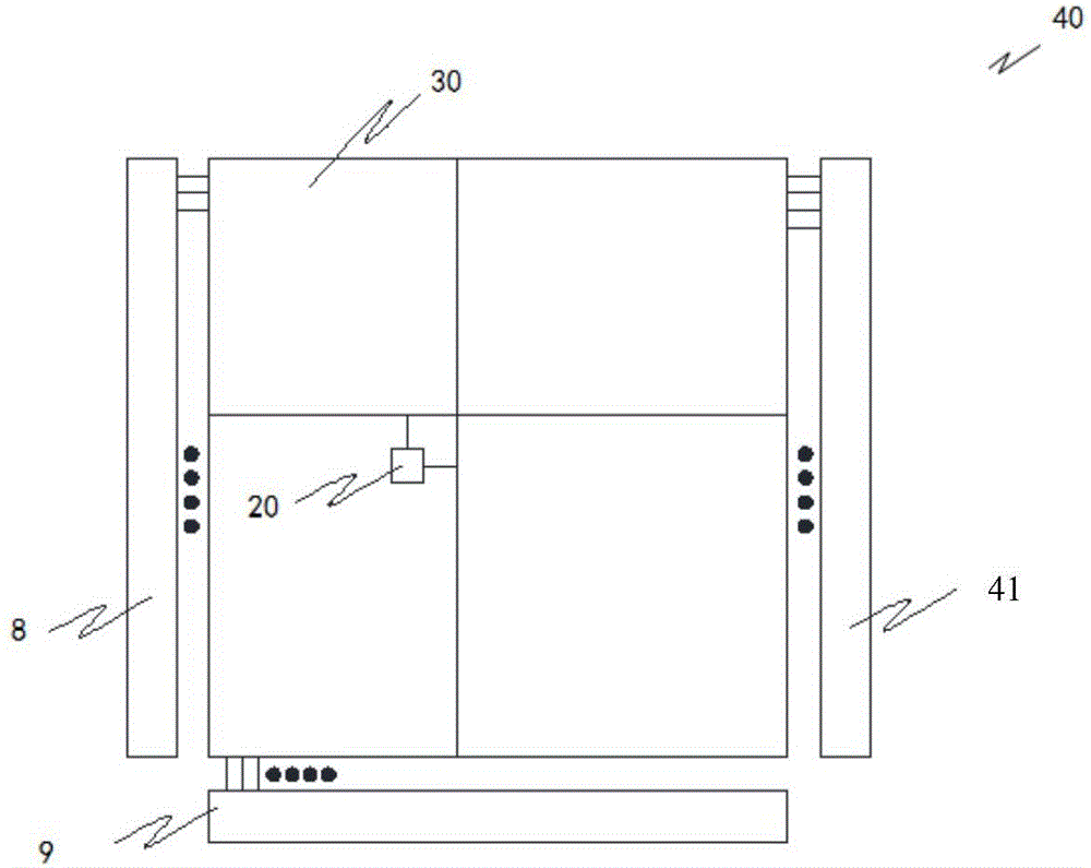
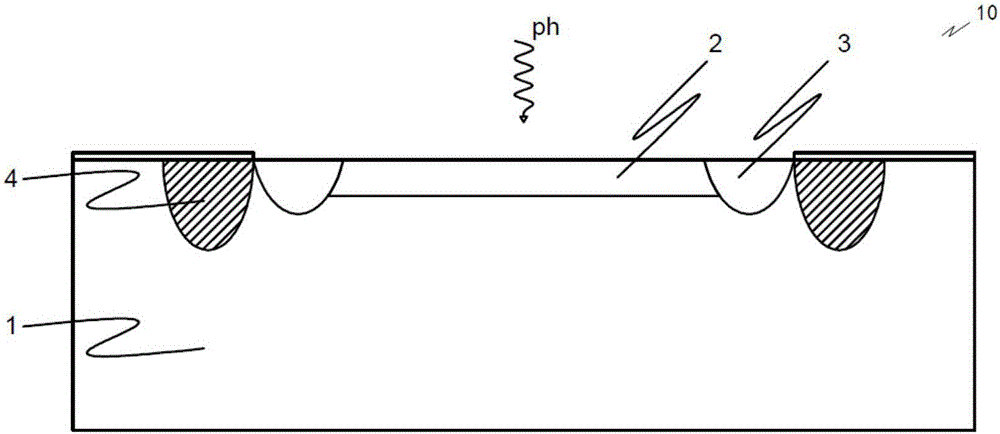
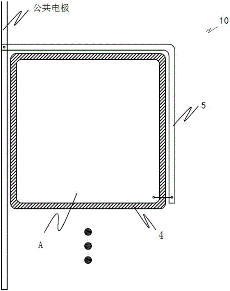
[0059] Such as figure 1 and figure 2 As shown, the present invention first discloses an avalanche breakdown photosensitive pixel unit 10 with high internal amplification gain and single photon sensitivity, comprising: a semiconductor substrate (not shown), an epitaxial layer formed on the semiconductor substrate . An avalanche photodiode formed in the above-mentioned epitaxial layer, the avalanche photodiode operates in a breakdown state and includes a drift region (not shown, located below the amplification region) for photon detection and an amplification region also for photon detection area, and a quenching unit 5 (passive or active form), which is connected in series with the avalanche photodiode. When the avalanche breakdown photosensitive pixel unit 10 detects a photon and causes an avalanche breakdown of the avalanche photodiode, the quenching unit 5 will terminate the avalanche process, so that the avalanche breakdown photosensitive pixel unit 10 returns to the init...


PUM


Abstract

The present invention discloses a digital semiconductor photoelectric magnification image sensor which comprises a digital semiconductor photosensitive pixel array for detecting a photon, an address unit which is connected to each digital semiconductor photosensitive pixel unit so as to determine the address information of each digital semiconductor photosensitive pixel unit in the array, a control unit which communicates with and is connected to the address unit to enable the digital semiconductor photosensitive pixel unit of a specified address and send corresponding data and address output command, and an output unit which communicates with and is connected to each digital semiconductor photosensitive pixel unit to transmit the data emitted by the digital semiconductor photosensitive pixel units and the corresponding address information after the digital semiconductor photosensitive pixel unit of the specified address is enabled. The sensor can output information that whether the photon is detected and the position information of the detected photon and thus can be widely used in a digital photoelectric imaging system.

Description

technical field [0001] The invention relates to a photodetection device for photon detection, in particular to a digitized semiconductor photoelectric image sensor. Background technique [0002] Low-throughput photon detection is used in many fields, such as medical imaging systems, especially positron emission tomography (PET), homeland security, high-energy physics experiments, and other critical areas of imaging. For low-throughput photon detection, conventional photomultiplier tubes (PMTs) and their associated hybrid photon detectors (HPDs) are generally used. These techniques have many advantages such as high gain (10 6 or higher), better linearity and lower dark current, but these traditional photodetectors also have some obvious disadvantages, such as larger size, higher operating voltage, sensitivity to magnetic field, complex manufacturing technology and high cost. Avalanche photodiodes can achieve linear amplification over a wide dynamic range, but the gain is l...

Claims


Application Information

Patent Timeline
Patent Type & Authority Applications(China)
IPC IPC(8): H01J43/04H01L31/02
Inventor N·达申佐V·萨维里耶夫王麟谢庆国
Owner WUHAN JOINBON TECH CO LTD
Why Eureka
Try Eureka