

High-resistance substrate for high-electron-mobility transistor and growing method thereof
A high electron mobility, transistor technology, applied in the direction of circuits, electrical components, semiconductor devices, etc., can solve the problems of deteriorating electrical properties of devices, crystal quality degradation, and no withstand voltage, so as to achieve excellent crystal quality and reduce lattice distortion. Effect
- Summary
- Abstract
- Description
- Claims
- Application Information
AI Technical Summary
Problems solved by technology
Method used
Image

Examples
Embodiment Construction
[0021] The specific implementation of the high-resistance substrate for high electron mobility transistors and the growth method provided by the present invention will be described in detail below with reference to the accompanying drawings.
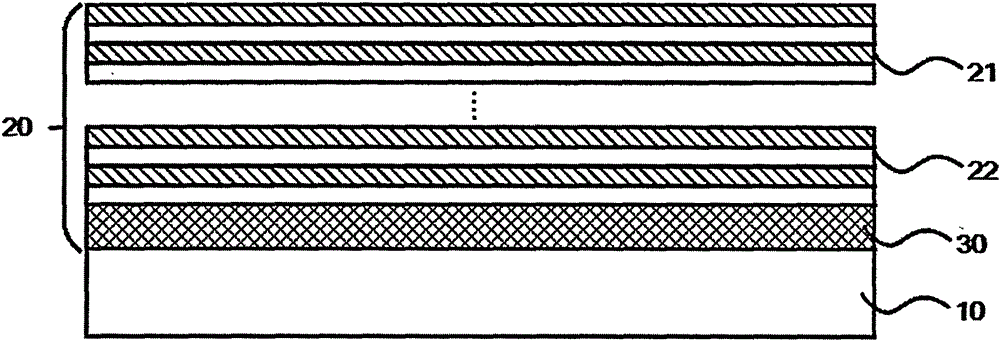
[0022] Reference attached figure 1 Shown is a schematic structural view of the high-resistance substrate for high electron mobility transistors described in this specific embodiment, including a support substrate 10 and a high-resistance layer 20 on the surface of the support substrate 10 . The material of the high resistance layer 20 is nitride. The high-resistance layer 20 includes a periodic structure in which a plurality of doped layers 21 and a plurality of non-doped layers 22 are arranged alternately. The multiple doped layers 21 and the multiple undoped layers 22 included in the high resistance layer 20 are all nitride materials, and the material of the doped layers 21 is nitride containing deep level doping elements. Deep-level...
PUM
| Property | Measurement | Unit |
|---|---|---|
| Doping concentration | aaaaa | aaaaa |
Abstract
Description
Claims
Application Information