
Analysis method of total dose effect sensitivity of logic gate circuit and analysis method of total dose effect sensitivity of CMOS digital circuit

A logic gate circuit and total dose effect technology, which is applied in the direction of circuit, electrical components, semiconductor/solid-state device testing/measurement, etc., can solve the problems of increased layout area, lack of screening methods, and reduced integration, so as to simplify the analysis process, Facilitate automatic operation and save layout area

Inactive Publication Date: 2015-11-18
NORTHWEST INST OF NUCLEAR TECH
View PDF4 Cites 2 Cited by
  • Summary
  • Abstract
  • Description
  • Claims
  • Application Information

AI Technical Summary

Problems solved by technology

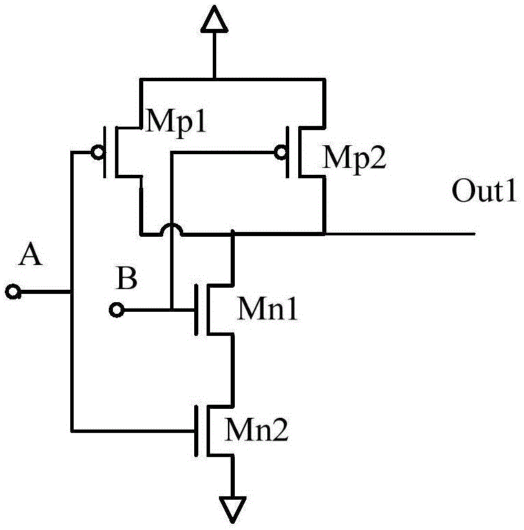
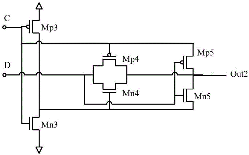
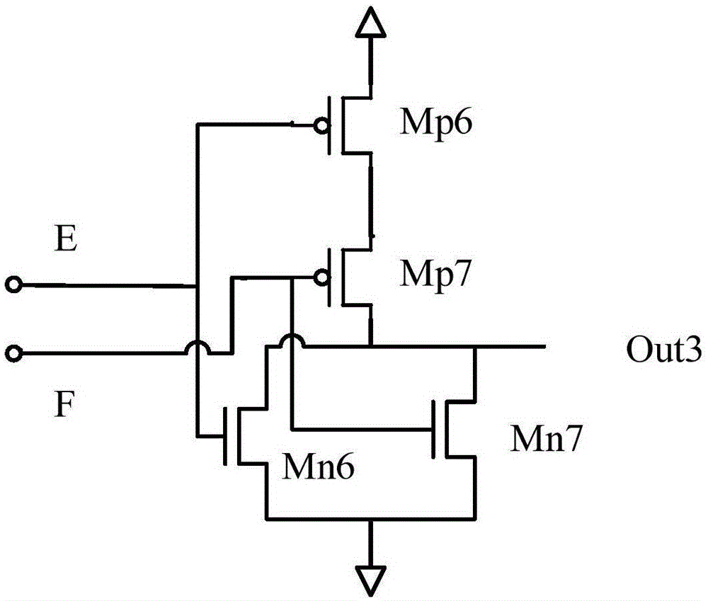
[0005] Aiming at the lack of existing methods for identifying sensitive areas of CMOS circuits, the existing reinforcement methods do not perform the identification of sensitive areas before the total dose of the circuit is strengthened, resulting in the increase of layout area and the reduction of indicators such as integration, the present invention provides a The analysis method for the sensitivity of the total dose effect of logic gate circuits and CMOS digital circuits can identify the sensitive nodes of the total dose effect, which can be used to guide the reinforcement design and obtain the balance between cost and radiation resistance performance

Method used


Image

  • Analysis method of total dose effect sensitivity of logic gate circuit and analysis method of total dose effect sensitivity of CMOS digital circuit
  • Analysis method of total dose effect sensitivity of logic gate circuit and analysis method of total dose effect sensitivity of CMOS digital circuit
  • Analysis method of total dose effect sensitivity of logic gate circuit and analysis method of total dose effect sensitivity of CMOS digital circuit

Examples


Embodiment Construction

[0029] The present invention will be described in detail below.

[0030] For the current general-purpose deep submicron or nanometer process integrated circuits, the total dose damage mainly affects the nMOS tubes, especially the nMOS tubes connected to high levels during the irradiation process, and the corresponding electrical characteristics of the pMOS tubes drift Almost negligible. Based on this consideration, when screening the total dose sensitivity of the circuit, it is only necessary to examine the combined state of high-level input signals during the irradiation process, and the combination of low-level input signals during the irradiation process can be directly eliminated .

[0031] The total dose damage of CMOS circuits is mainly characterized by the gradual decrease of the output high level value with the increase of the cumulative dose. When the amplitude of the output high level is low to a certain extent, it may be misidentified as a logic low level by the ba...


PUM


Abstract

The invention relates to an analysis method of a total dose effect sensitivity of a logic gate circuit and an analysis method of a total dose effect sensitivity of a CMOS digital circuit. The analysis method of the total dose effect sensitivity of the logic gate circuit comprises 1) listing a working state of a to-be-analyzed logic gate circuit in an irradiation process, listing a working state of the to-be-analyzed logic gate circuit in a test process, and performing permutation and combination on the working states in the two processes to form multiple groups of input signal combinations, 2) simplifying a specific structure of a pMOS tube combination and a specific structure of an nMOS tube combination which form the logic gate circuit, and enabling the specific structure of the pMOS tube combination and the specific structure of the nMOS tube combination to be equivalent to structure forms of phase inverters, and 3) calculating electric conductance of the various phase inverters, wherein a combination of the minimum equivalent pMOS tube electric conductance and the maximum equivalent nMOS tube electric conductance corresponds to the strongest total-dose sensitivity. The method capable of rapidly identifying total-dose effect sensitive nodes in a circuit achieves identification of the total-dose effect sensitive nodes in the circuit during the design phase, and then can be used to guide reinforcing design and greatly save the layout area.

Description

technical field [0001] The invention belongs to the research field of total dose effect of CMOS digital integrated circuits. Background technique [0002] Semiconductor device circuits working in the space radiation environment for a long time will be affected by the total dose effect, which is specifically characterized by the degradation of the electrical performance of the device or circuit or even functional failure. [0003] Common methods for total dose hardening of circuits can be divided into three categories: layout hardening, design hardening, and shield hardening. Layout reinforcement refers to the adjustment of the most basic unit, such as changing the ion implantation in the process flow, changing the position or number of well contacts, changing the layout structure of a single tube, etc., see patent application number 201010548221.4, "An anti-total dose radiation hardened transistor structure", etc. Design hardening refers to adjustments at the netlist level...

Claims


Application Information

Patent Timeline
IPC IPC(8): H01L21/60
CPCH01L22/30
Inventor 丁李利郭红霞陈伟姚志斌郭晓强罗尹虹张凤祁赵雯
Owner NORTHWEST INST OF NUCLEAR TECH
Learn More