

Semiconductor structure forming method
A semiconductor and plasma technology, used in semiconductor/solid-state device manufacturing, electrical components, circuits, etc., can solve problems affecting the performance of fin field effect transistors, blocking ion implantation, and affecting the effect of lightly doped ion implantation.
- Summary
- Abstract
- Description
- Claims
- Application Information
AI Technical Summary
Problems solved by technology
Method used
Image

Examples
Embodiment Construction
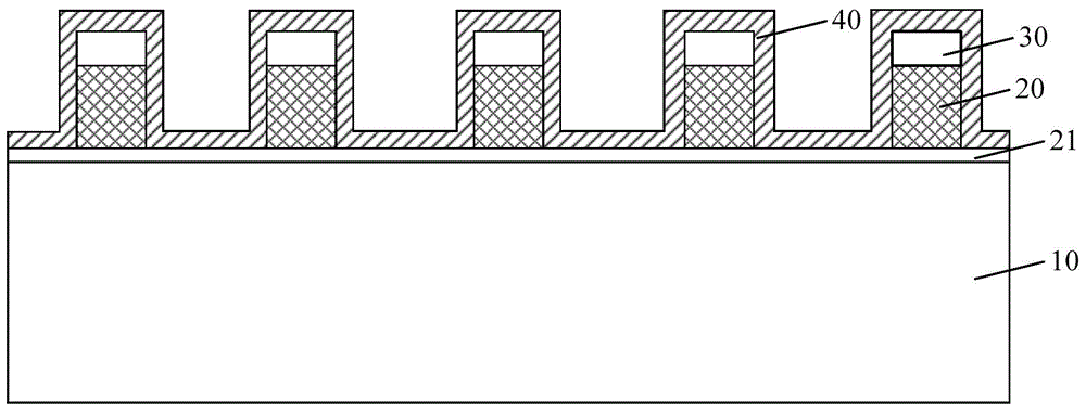
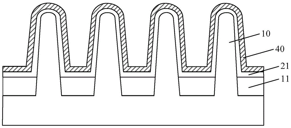
[0030] As mentioned in the background technology, when forming the sidewall on the sidewall surface of the gate structure of the fin field effect transistor, the sidewall material layer on the sidewall surface of the fin is difficult to remove, which will cover the surface of the fin and affect the thickness Ion implantation is performed on the fin, thereby affecting the performance of the formed fin field effect transistor.
[0031] One embodiment of the present invention provides a method of removing a layer of sidewall material on a sidewall of a fin.
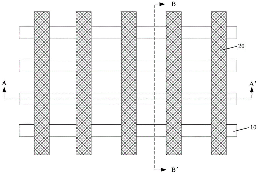
[0032] Please refer to figure 1 , forming several fins 10 arranged in parallel on the semiconductor substrate; forming an isolation layer on the surface of the semiconductor substrate, the surface of the isolation layer is lower than the top surface of the fins 10; forming a gate across the fins electrode 20, the top of the gate has a mask layer. figure 1 It is a schematic plan view after omitting the semiconductor subst...
PUM
 Abstract
Description
Claims
Application Information