UTB-SOI tunneling field-effect transistor with abrupt junction and preparation method thereof

A technology of UTB-SOI and tunneling field effect, which is applied in semiconductor/solid-state device manufacturing, semiconductor devices, electrical components, etc., can solve the problems of subthreshold slope theoretical value degradation and small driving current, and achieve high practical value and improve performance effect

Inactive Publication Date: 2015-12-02
XIAN UNIV OF SCI & TECH
View PDF3 Cites 19 Cited by
  • Summary
  • Abstract
  • Description
  • Claims
  • Application Information

AI Technical Summary

Problems solved by technology

[0005] In order to overcome the problems of low driving current of existing silicon-based TFET devices and the degradation of subthreshold slope relati

Method used


Image

  • UTB-SOI tunneling field-effect transistor with abrupt junction and preparation method thereof
  • UTB-SOI tunneling field-effect transistor with abrupt junction and preparation method thereof
  • UTB-SOI tunneling field-effect transistor with abrupt junction and preparation method thereof

Examples


Embodiment 1

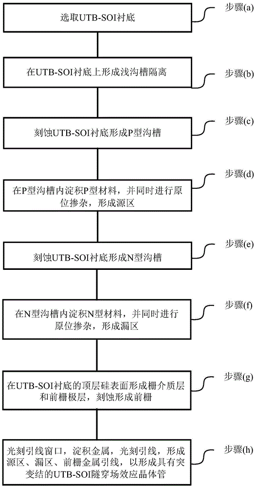
[0060] See figure 1 with Figure 2a-Figure 2i , figure 1 It is a flow chart of a method for preparing an N-type UTB-SOI tunneling field-effect transistor with an abrupt junction according to an embodiment of the present invention, Figure 2a-Figure 2i It is a schematic diagram of a preparation method of an N-type UTB-SOI tunneling field effect transistor with an abrupt junction according to an embodiment of the present invention, and the preparation method includes the following steps:

[0061] (a) Select Ultra-Thin-Body-Silicon-On-Insulator (UTB-SOI for short) substrate;

[0062] (b) forming shallow trench isolation on the UTB-SOI substrate;

[0063] (c) Etching the UTB-SOI substrate to form a P-type trench;

[0064] (d) Depositing the material of the source region and performing in-situ doping on the source region at the same time to form a highly doped P-type source region.

[0065] (e) Etching the UTB-SOI substrate to form an N-type trench;

[0066] (f) Depositing the ...

Embodiment 2

[0101] See image 3 , image 3 It is a schematic flow chart of a method for preparing a UTB-SOI tunneling field-effect transistor with an abrupt junction according to an embodiment of the present invention, taking the preparation of an N-type UTB-SOI tunneling field-effect transistor with an abrupt junction with a channel length of 45 nm as an example. In detail, the specific steps are as follows:

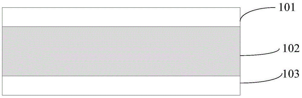
[0102] 1. Select UTB-SOI substrate

[0103] The crystal orientation of the UTB-SOI substrate 101 may be (100) or (110) or (111), without any limitation here. In addition, the doping type of the UTB-SOI substrate 101 may be N type, or It can be P-type, and the doping concentration is, for example, 10 14 ~10 17 cm -3 , the thickness of the top layer Si is, for example, 10-20 nm.

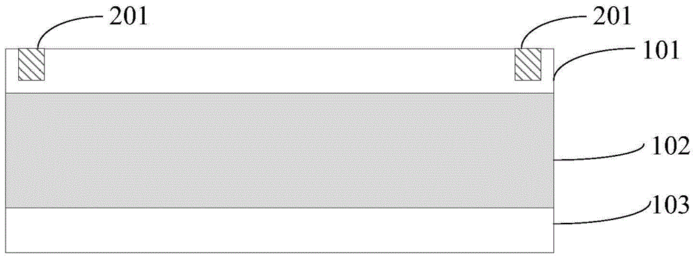
[0104] 2. Shallow trench isolation formation

[0105] 2.1 Form a first protective layer on the UTB-SOI substrate.

[0106] First, two layers of materials are continuously grown on the UTB-SOI substr...

Embodiment 3

[0167] See Figure 4 , Figure 4 It is a schematic diagram of the device structure of a UTB-SOI tunneling field effect transistor with an abrupt junction according to an embodiment of the present invention. The UTB-SOI tunneling field effect transistor with an abrupt junction of the present invention includes an ultra-thin top silicon layer, a buried oxide layer, underlying silicon layer, gate dielectric layer, front gate, back gate, highly doped source region and low doped drain region.

[0168] Specifically, the thickness of the ultra-thin top silicon layer is preferably 10-20 nm, and the doping concentration is less than 10 17 cm -3 .

[0169] Specifically, the material of the gate dielectric layer can be selected from hafnium-based materials (a type of high dielectric constant material), such as HfO 2 , HfSiO, HfSiON, HfTaO, HfTiO or HfZrO or a combination thereof, other high dielectric constant materials such as Al 2 o 3 , La 2 o 3 , ZrO 2 Or one or a combination...


PUM

PropertyMeasurementUnit
Thicknessaaaaaaaaaa
Thicknessaaaaaaaaaa
Thicknessaaaaaaaaaa

Abstract

The invention relates to an ultra-thin-body-silicon-on-insulator (UTB-SOI) tunneling field-effect transistor with an abrupt junction and a preparation method thereof. The preparation method comprises: selecting a UTB-SOI substrate; forming a shallow trench isolation unit; carrying out etching to form a P type/N type trench; carrying out silicon material deposition in the P type/N type trench and carrying out in-situ doping to form a P type/N type highly-doped source region; carrying out etching to form an N type/P type trench; carrying out silicon material deposition in the N type/P type trench and carrying out in-situ doping to form a low doped N type/P type drain region; forming a gate dielectric layer and a front gate layer on the top layer silicon surface of the substrate and carrying out etching to form a front gate; and carrying out lead window photoetching, metal deposition, and lead photoetching to form source region, drain region, and front gate metal leads. According to the invention, with the technique and preparation of trench etching and selective epitaxy deposition and filling at the source and drain regions, the tunnel junction area can be limited precisely; and on the basis of in-situ doping, the tunnel junction with the steep doping concentration gradient and the source and drain regions with uniform doping can be formed well and the driving current of the device can be effectively improved and the sub-threshold slope can be reduced.

Description

technical field [0001] The invention belongs to the technical field of semiconductor integrated circuits, and in particular relates to a UTB-SOI tunneling field effect transistor with an abrupt junction and a preparation method. Background technique [0002] Integrated Circuit (IC for short) technology follows the development of "Moore's Law" and has entered the nanoscale. Challenges from short channel effects, parasitic effects, and quantum tunneling make it increasingly difficult for traditional microelectronic device technology to meet the requirements of IC. The requirement of continuous technological development, especially the increasingly serious power consumption problem, has become the biggest bottleneck in continuing "Moore's Law". [0003] Tunneling Field Effect Transistor (Tunneling Field Effect Transistor, referred to as TFET) adopts the physical mechanism of band-band tunneling, so that its sub-threshold swing is not limited by the limit value KT / q of the tradi...

Claims


Application Information

Patent Timeline
IPC IPC(8): H01L21/336H01L21/762H01L21/28H01L29/78H01L29/08H01L29/423
CPCH01L21/7624H01L29/0847H01L29/401H01L29/4232H01L29/66484H01L29/7831
Inventor 李妤晨童军刘树林张岩徐大庆张超岳改丽刘宁庄杨波秦学斌
Owner XIAN UNIV OF SCI & TECH
Why Eureka
Try Eureka