Thin film transistor biosensor and preparation method thereof
A technology of thin-film transistors and biosensors, which is applied in the field of semiconductor technology and biochemistry, can solve problems such as the impact of transistor service life, and achieve the effect of increasing stability and service life
- Summary
- Abstract
- Description
- Claims
- Application Information
AI Technical Summary
Problems solved by technology
Method used
Image
Examples
preparation example Construction
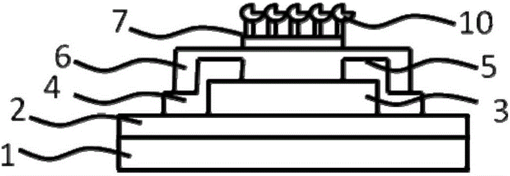
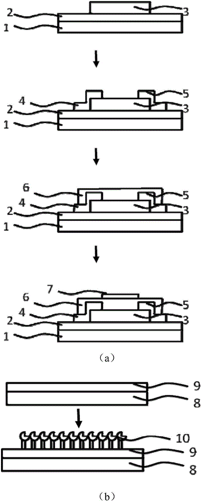
[0039] image 3 It is a flow chart of the preparation method of the thin film transistor biosensor of the present invention, such as image 3 Shown, this preparation method comprises:
[0040] Step S1: Preparation of Thin Film Transistor
[0041] Select n-type thermal oxide silicon wafer as the substrate;
[0042] Depositing a semiconductor channel layer 3 on the surface of the substrate by using a magnetron sputtering deposition method;
[0043] Depositing a source electrode 4 and a drain electrode 5 on the surface of the semiconductor channel layer by using electron beam evaporation coating equipment;
[0044] Depositing a cover layer 6 on the surface of the source electrode 4, the drain electrode 5 and the surface of the semiconductor channel layer 3 by using electron beam evaporation coating equipment;
[0045] The first conductive thin film 7 is deposited on the surface of the covering layer by electron beam evaporation coating equipment; then annealing treatment is p...
Embodiment 1
[0054] (1) Preparation of IGZO thin film transistors:
[0055] (1.1) Select an n-type heavily doped thermally oxidized silicon wafer (the thickness of the thermal oxide layer is about 112nm) with a 100 crystal orientation as the substrate, and clean and dry it.
[0056] (1.2) A magnetron sputtering deposition method is used to deposit an IGZO thin film on the surface of the thermal oxide layer as a semiconductor channel layer. Among them, the working gas used is a mixed gas of argon and oxygen (Ar:O 2 =14:3); the sputtering power is 100W; the gas pressure is 0.9Pa; the deposition temperature is room temperature. The thickness of the finally prepared IGZO film is 48nm, and the length and width are 400μm and 800μm, respectively.
[0057] (1.3) Electron beam evaporation coating equipment and granular metal Ti and Au evaporation coating materials are used to prepare Ti / Au source and drain electrodes by mask method. The thickness of the source electrode and the drain electrode p...
Embodiment 2
[0067] (1) Preparation of IGZO thin film transistor: as in Example 1.
[0068] (2) Preparation of biosensors:
[0069] (2.1) Select an n-type silicon wafer with a 100 crystal orientation as a solid phase carrier, perform ultrasonic cleaning with acetone, alcohol, and deionized water for 5 minutes, and blow dry with nitrogen.
[0070] (2.2) Electron beam evaporation coating equipment and granular metal Ni / Au evaporation coating materials are used to prepare Ni / Au films. In this embodiment, the deposited film thickness is Ni / Au=50:20 nm.
[0071] (2.3) Goat anti-mouse IgG biomolecules were modified on the surface of Au membrane by covalent bond method. The sensing area was immersed in 16mMAET solution, the surface was thiolated (5h), and then washed with deionized water. The sensing area was immersed in GTDA (5%, v / v) solution for hydroformylation (2 h), and then washed with deionized water. Add 10ug / ml goat anti-mouse IgG dropwise on the surface of the sensing area, seal it...
PUM
| Property | Measurement | Unit |
|---|---|---|
| Thickness | aaaaa | aaaaa |
| Thickness | aaaaa | aaaaa |
| Thickness | aaaaa | aaaaa |
Abstract
Description
Claims
Application Information
 - R&D Engineer
- R&D Manager
- IP Professional
- Industry Leading Data Capabilities
- Powerful AI technology
- Patent DNA Extraction
Browse by: Latest US Patents, China's latest patents, Technical Efficacy Thesaurus, Application Domain, Technology Topic, Popular Technical Reports.
© 2024 PatSnap. All rights reserved.Legal|Privacy policy|Modern Slavery Act Transparency Statement|Sitemap|About US| Contact US: help@patsnap.com


