Organic bulk heterojunction photoresistor and preparation method thereof

A phototransistor and heterojunction technology, applied in photovoltaic power generation, semiconductor/solid-state device manufacturing, circuits, etc., can solve the problems of low flexibility, high cost, high power consumption, etc. The effect of stretching and reducing the working voltage

Active Publication Date: 2015-12-09
SHENZHEN UNIV
View PDF4 Cites 16 Cited by
  • Summary
  • Abstract
  • Description
  • Claims
  • Application Information

AI Technical Summary

Problems solved by technology

[0003] In view of the above-mentioned deficiencies in the prior art, the purpose of the present invention is to provide an organic heterojunction phototransistor and its preparation method, aiming to solve the problems of high power consumption, low sensitivity, high cost and low flexibility of existing phototransistors

Method used


Image

  • Organic bulk heterojunction photoresistor and preparation method thereof
  • Organic bulk heterojunction photoresistor and preparation method thereof
  • Organic bulk heterojunction photoresistor and preparation method thereof

Examples


Embodiment Construction

[0027] The present invention provides an organic heterojunction phototransistor and its preparation method. In order to make the purpose, technical solution and effect of the present invention clearer and clearer, the present invention will be further described in detail below. It should be understood that the specific embodiments described here are only used to explain the present invention, not to limit the present invention.

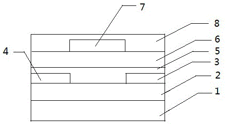
[0028] see figure 1 , figure 1 It is a schematic structural diagram of a preferred embodiment of an organic heterojunction phototransistor of the present invention, as shown in the figure, which includes: a substrate 1, a flexible material layer 2 arranged on the substrate 1, and a flexible material layer 2 on the flexible material The drain electrode 4 and the source electrode 3 arranged at both ends on the layer 2, the active layer 5 arranged on the drain electrode 4, the source electrode 3 and the non-covered electrode area on the flexible materia...


PUM


Abstract

The invention discloses an organic bulk heterojunction photoresistor and a preparation method thereof. According to the invention, an organic bulk heterojunction formed by an electron donor material and an electron acceptor material through solution blending is adopted to act as an active layer material system. When the new material system is applied to an organic bulk heterojunction photoresistor, the photoelectric responsivity and the tensibility of the organic bulk heterojunction photoresistor can be enabled to be significantly improved, and the operating voltage can be enabled to be reduced.

Description

technical field [0001] The invention relates to the technical field of phototransistors, in particular to an organic heterojunction phototransistor and a preparation method thereof. Background technique [0002] Among various photodetector structures, phototransistors have the characteristics of high sensitivity and adjustable optical gain. Conventional phototransistors are fabricated from Group IV silicon (Si) or Group III-V inorganic semiconductor materials. According to reports, the photoresponsivity of inorganic phototransistors made of indium gallium arsenide (InGaAs) materials is as high as 400AW -1 . However, inorganic phototransistors need to be prepared by high-temperature, high-cost electronic epitaxy growth process, and the material is hard, which limits the wide application of this type of phototransistor (such as the field of wearable devices). Recently, organic and nano-semiconductor materials have become research hotspots at home and abroad. These materials...

Claims


Application Information

Patent Timeline
Patent Type & Authority Applications(China)
IPC IPC(8): H01L51/42H01L51/48
CPCH10K30/354H10K30/65H10K30/30Y02E10/549
Inventor 徐海华程正喜张会生邓永春
Owner SHENZHEN UNIV
Why Eureka
Try Eureka