GaAs (111) wafer cleaning method

A wafer, hydrochloric acid technology, applied in the direction of electrical components, semiconductor/solid-state device manufacturing, circuits, etc., can solve the problems of destroying the surface morphology of the substrate, irregular natural oxide layer, and inability to obtain effects.

Inactive Publication Date: 2015-12-16
GUILIN UNIV OF ELECTRONIC TECH
View PDF5 Cites 4 Cited by
  • Summary
  • Abstract
  • Description
  • Claims
  • Application Information

AI Technical Summary

Problems solved by technology

However, the method of treating GaAs surface with hydrochloric acid solution alone cannot obtain the desired effect.
The main reason is that the natural oxide layer on the surface of GaAs is irregular, and the hydrochloric acid solution also reacts with GaAs while corroding the oxide, thus destroying the morphology of the substrate surface and increasing the surface roughness of the material.

Method used


Image

  • GaAs (111) wafer cleaning method
  • GaAs (111) wafer cleaning method
  • GaAs (111) wafer cleaning method

Examples


Embodiment 1

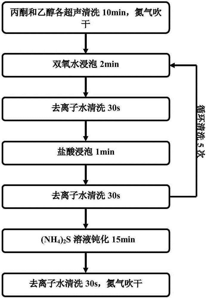
[0032] 1) The GaAs(111)A substrate was ultrasonically cleaned with acetone and ethanol in sequence, and the ultrasonic time was 10 minutes to remove oil and organic matter on the substrate surface;

[0033]2) Soak the substrate obtained in step 1) in hydrogen peroxide with a mass concentration of 30% for 2 minutes, take it out, and wash it in deionized water for 30 seconds; after taking it out, soak it in hydrochloric acid with a mass concentration of 10% for 1 min , take it out, wash it in deionized water for 30s, take out the substrate and repeat the steps of soaking in hydrogen peroxide—cleaning in deionized water—soaking in hydrochloric acid—cleaning in deionized water 4 times (that is, soaking in hydrogen peroxide—cleaning in deionized water—soaking in hydrochloric acid—deionized water Cleaning step cycle 5 times), after completing the last deionized water cleaning, blow dry with nitrogen;

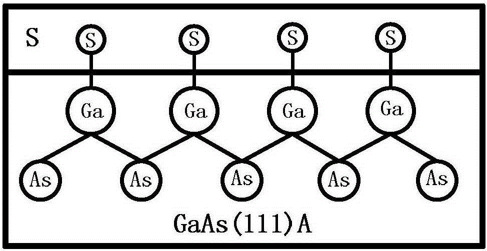
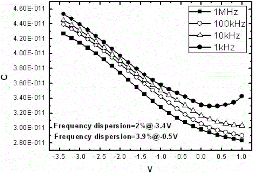
[0034] 3) Place the GaAs(111) substrate obtained after the treatment in step 2) i...

Embodiment 2

[0042] 1) The GaAs(111)B substrate is ultrasonically cleaned with acetone and ethanol in sequence, and the ultrasonic time is 5 minutes and 15 minutes respectively, to remove oil and organic matter on the surface of the substrate;

[0043] 2) Soak the substrate obtained in step 1) in hydrogen peroxide with a mass concentration of 25% for 3 minutes, take it out, and wash it in deionized water for 30 seconds; after taking it out, soak it in hydrochloric acid with a mass concentration of 13% for 2 minutes, take it out , wash in deionized water for 30s, take out the substrate and repeat the steps of soaking in hydrogen peroxide-cleaning in deionized water-soaking in hydrochloric acid-cleaning in deionized water twice, after the last deionized water cleaning, blow dry with nitrogen;

[0044] 3) Place the GaAs(111) substrate obtained after the treatment in step 2) in (NH 4 ) 2 Passivate in S solution for 20 minutes, take it out, wash it in deionized water for 30 seconds, and dry it...

Embodiment 3

[0047] 1) The GaAs(111)A substrate was ultrasonically cleaned with acetone and ethanol in sequence, and the ultrasonic time was 10 minutes to remove oil and organic matter on the substrate surface;

[0048] 2) Soak the substrate obtained in step 1) in hydrogen peroxide with a mass concentration of 35% for 5 minutes, take it out, and wash it in deionized water for 30 seconds; after taking it out, soak it in hydrochloric acid with a mass concentration of 8% for 3 minutes, take it out , wash in deionized water for 60s, take out the substrate and repeat the steps of soaking in hydrogen peroxide-cleaning in deionized water-soaking in hydrochloric acid-cleaning in deionized water 3 times, after the last deionized water cleaning, blow dry with nitrogen;

[0049] 3) Place the GaAs(111) substrate obtained after the treatment in step 2) into (NH 4 ) 2 Passivate in S solution for 10 minutes, take it out, wash it in deionized water for 30 seconds, and dry it with nitrogen.


PUM


Abstract

The invention discloses a GaAs (111) wafer cleaning method. The GaAs (111) wafer cleaning method comprises steps that, a GaAs (111) substrate is treated by an organic solvent to remove oil stain and organic matters on the surface; the GaAs (111) substrate is immersed in hydrogen peroxide, is then taken out, is cleaned by deionized water, is immersed in hydrochloric acid, is taken out and is cleaned by deionized water; the acquired GaAs (111) substrate is immersed in hydrogen peroxide, is cleaned by deionized water, is immersed in hydrochloric acid and is cleaned by deionized water for at least one time. According to the method, the surface of the GaAs (111) substrate is treated by the hydrogen peroxide to acquire a structured nature oxide layer and is then corroded by the hydrochloric acid, as the GaAs (111) surface is the structured nature oxide layer, GaAs defects with bad quality in the surface can be effectively removed, so oxide quantity and roughness of the GaAs surface can be greatly reduced. The cleaning method is employed in combination with an ammonium sulphide solution for passivation, so the clean GaAs surface can be prevented from being oxided by oxygen in the air for long time.

Description

technical field [0001] The invention relates to the preparation of GaAsMOSCAP (MOS capacitor), in particular to a method for cleaning a GaAs (111) wafer. Background technique [0002] In recent years, with the continuous breakthrough of semiconductor technology nodes, the requirements for device size have become more stringent, and further reducing the physical size of devices according to conventional methods has been challenged in many ways. People began to look for new materials to replace Si. Among them, GaAs and other III-V compound semiconductor materials have attracted extensive attention due to their high electron mobility and critical field strength. However, oxides of III-V compound semiconductor materials cannot compare with SiO in terms of stability and quality. 2 In contrast, this seriously affects the performance of III-V compound semiconductor field effect transistors, so people use high-K dielectrics instead of their oxides as gate dielectric materials, and ...

Claims


Application Information

Patent Timeline
Patent Type & Authority Applications(China)
IPC IPC(8): H01L21/02
CPCH01L21/02052
Inventor 李海鸥林子曾曹明民王盛凯刘洪刚李琦肖功利高喜曹卫平
Owner GUILIN UNIV OF ELECTRONIC TECH
Why Eureka
Try Eureka