
LED epitaxial structure having combination barrier multi-quantum well and preparation method

A multi-quantum well structure and multi-quantum well technology, which is applied in the field of high-brightness LED epitaxial structure and its preparation, can solve the problems of large stress and low quantum efficiency, and achieve the effects of reducing stress, improving device performance, and alleviating bending

Inactive Publication Date: 2015-12-16
SHANDONG INSPUR HUAGUANG OPTOELECTRONICS
View PDF5 Cites 23 Cited by
  • Summary
  • Abstract
  • Description
  • Claims
  • Application Information

AI Technical Summary

Problems solved by technology

[0010] The present invention aims at the problems of low quantum efficiency and large stress in existing multi-quantum wells, and provides an LED epitaxial structure with combined potential barrier multi-quantum wells, which can effectively reduce the stress between well-barrier interfaces and ease the bending of energy bands , improve the efficiency of hole and electron injection into the active region and the efficiency of radiative recombination

Method used


Image

  • LED epitaxial structure having combination barrier multi-quantum well and preparation method
  • LED epitaxial structure having combination barrier multi-quantum well and preparation method

Examples


Embodiment Construction

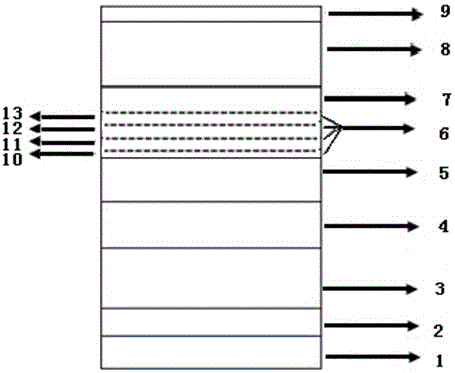
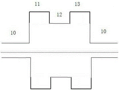
[0043] Such as figure 1 As shown, the present invention has a high-brightness base LED epitaxial structure with combined potential barriers and multiple quantum wells, and is provided with a substrate layer 1, a GaN buffer layer 2, an undoped GaN layer 3, an n-type AlGaN layer 4, and an n-type AlGaN layer from bottom to top. Type GaN layer 5, multi-quantum well active light-emitting layer 6, P-type AlGaN layer 7, P-type GaN layer 8 and P-type InGaN ohmic contact layer 9. The substrate is sapphire. The thickness of the GaN buffer layer is 20-40nm. The thickness of the non-doped GaN layer is 2-3 μm. The thickness of the n-type AlGaN layer is 30-60 nm. The thickness of the n-type GaN layer is 2-3 μm. The thickness of the P-type AlGaN layer is 50-100 nm. The thickness of the P-type layer is 150-300nm. The thickness of the P-type ohmic contact layer is 2-10 nm. The multi-quantum well active light-emitting layer 6 is a combined barrier. The multi-quantum well layer is compose...


PUM


Abstract

The invention discloses an LED epitaxial structure having a combination barrier multi-quantum well and a preparation method. An active layer of the LED expitaxial structure is a combination barrier multi-quantum well structure, which are obtained through periodically stacking an InGaN potential well, an InAlGa barrier well, a GaN barrier layer and an InAlGa barrier layer. The preparation method comprises steps of (1) performing nitridation treatment on a sapphire substrate, (2) successively growing a CaN buffer layer, a non-doping CaN layer, an n type AlGaN layer and an n type GaN layer, (3) growing a combination barrier multi-quantum well on the n type GaN layer which includes the steps of (A) growing an InxGa1-xN potential well layer, (B) growing an InaAlbGa1-a-bN layer, a Gan barrier layer and an InaAlbGa1-a-bN layer, wherein the period circulation times of the step (A) and the step (B) are 5-20, and the step (B) is a cycle loop or a multi-cycle, and (4) successively growing a P type layer on the combination barrier multi-quantum layer. The invention substantially improves the quality of the crystal and efficiency of the inner quantum, improves the performance of the member and improves the light out-coming efficiency by 10%.

Description

technical field [0001] The invention relates to a high-brightness based LED epitaxial structure with combined potential barrier multi-quantum wells capable of improving light extraction efficiency and a preparation method thereof, belonging to the technical field of LED epitaxial design. Background technique [0002] In the early 1990s, the third-generation wide-bandgap semiconductor materials represented by nitrides made a historic breakthrough. Researchers successfully prepared blue-green and ultraviolet LEDs on gallium nitride materials, making LED lighting become possible. In 1971, the first gallium nitride LED die came out. In 1994, gallium nitride HEMTs appeared blue light GaN-based diodes with high electron mobility, and gallium nitride semiconductor materials developed very rapidly. [0003] Semiconductor light-emitting diodes have the advantages of small size, ruggedness, strong controllability of light-emitting bands, high luminous efficiency, low heat loss, low l...

Claims


Application Information

Patent Timeline
IPC IPC(8): H01L33/06H01L33/32H01L33/00H01L21/205C23C16/44
CPCH01L33/06H01L21/2056H01L33/0066H01L33/0075H01L33/32
Inventor 张义曲爽逯瑶王成新徐现刚
Owner SHANDONG INSPUR HUAGUANG OPTOELECTRONICS
Learn More