Buried-channel SiC trench gate metal oxide semiconductor field effect transistors (MOSFETs) device and fabrication method thereof

A technology of silicon carbide trench and silicon carbide, which is applied in semiconductor/solid-state device manufacturing, semiconductor devices, electrical components, etc., can solve problems such as high threshold voltage and on-resistance, influence of effective electron mobility, and difficulty in practical use. Achieve the effect of avoiding high threshold voltage, avoiding low effective mobility, and improving effective mobility

Active Publication Date: 2015-12-23
GLOBAL ENERGY INTERCONNECTION RES INST CO LTD +2
View PDF5 Cites 7 Cited by
  • Summary
  • Abstract
  • Description
  • Claims
  • Application Information

AI Technical Summary

Problems solved by technology

The problem with this structure is that the threshold voltage and on-resistance of the device are too high, making it difficult to achieve a practical
This ion implantation process will negatively affect the effective mobility of electrons in the channel surface accumulation layer

Method used


Image

  • Buried-channel SiC trench gate metal oxide semiconductor field effect transistors (MOSFETs) device and fabrication method thereof
  • Buried-channel SiC trench gate metal oxide semiconductor field effect transistors (MOSFETs) device and fabrication method thereof
  • Buried-channel SiC trench gate metal oxide semiconductor field effect transistors (MOSFETs) device and fabrication method thereof

Examples


Embodiment 1

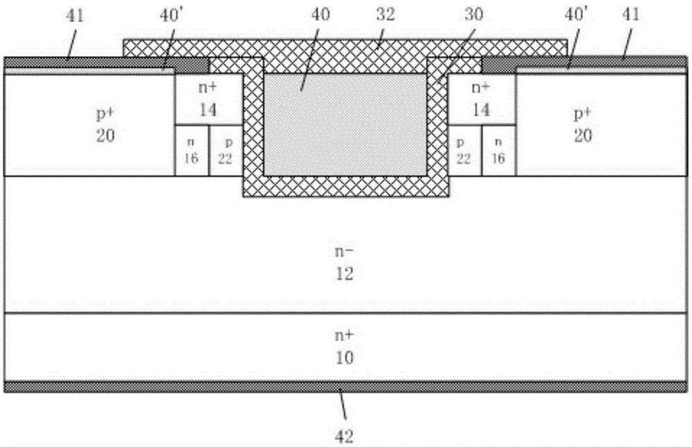
[0098] The device fabrication of the embodiment of the present invention can refer to Figure 4-13 description of.

[0099] in such as Figure 4 On the n-type silicon carbide substrate 10 shown and the n-type silicon carbide drift layer 12 thereon, an ion implantation mask is formed and patterned, and p-type doped impurity aluminum is implanted into the n-type layer 12 to form a Figure 5 P+ silicon carbide regions 20 are shown with spacing.

[0100] Such as Figure 6 As shown, an n+ silicon carbide source region 14 is formed on the p+ silicon carbide region 20 and the n-type silicon carbide drift layer 12 by making a masking film and patterning it and then ion-implanting nitrogen.

[0101] Such as Figure 7 As shown, the implantation of low-dose nitrogen-doped impurities is continued to provide n-type doped regions 16 between the p+-type silicon carbide regions 20 .

[0102] Such as Figure 8 As shown, polysilicon is deposited, polysilicon is etched, an implantation mas...

Embodiment 2

[0110] The device fabrication of the embodiment of the present invention can refer to Figure 14-17 and Figure 10-13 description of,

[0111] in such as Figure 14 On the n-type silicon carbide substrate 10 shown and the n-type silicon carbide drift layer 12, the n-type silicon carbide doped layer 16 and the n+ type silicon carbide doped layer 14 thereon, an ion implantation mask is formed and patterned , implanting p-type doped impurity aluminum, forming such as Figure 15 P+ silicon carbide regions 20 are shown with spacing.

[0112] Such as Figure 16 As shown, a p-type silicon carbide doped region 22 is formed on the p+ silicon carbide region 20 and the n+ type silicon carbide layer 14 by making a masking film and patterning it and implanting aluminum.

[0113] Such as Figure 17 As shown, silicon oxide is deposited, silicon oxide is etched, annealed to form an etching mask for the trench, silicon carbide is etched, and the surface of the n+ silicon carbide source r...


PUM


Abstract

The invention provides a buried-channel SiC trench gate metal oxide semiconductor field effect transistors (MOSFETs) device and a fabrication method thereof. The device comprises an n-type SiC substrate, n-type buried channels, p-type SiC regions, a trench medium, a gate contact, base region contacts, source contacts and a drain contact, wherein an n-type SiC drift layer is arranged on the substrate and internally comprises p<+>-type SiC regions at intervals, and n<+>-type SiC regions are arranged between the p<+>-type SiC regions; the n-type buried channels are arranged between the p<+>-type SiC regions and arranged in the n-type SiC drift layers under the n<+>-type SiC source regions; and the p-type SiC regions are arranged under the n<+>-type SiC source regions, are arranged in the n-type buried channels, and are opposite to the p<+>-type SiC regions. On the basis of a trench gate MOSFET structure, the buried channels provided for source and drain conductive passages are achieved by reversely doping a part of p well regions, the problems of low effective mobility of surface electrons and high threshold voltage are prevented, and a normally-closed device is achieved.

Description

technical field [0001] The invention relates to a semiconductor device and a manufacturing method thereof, in particular to a buried channel silicon carbide trench gate MOSFETs device and a manufacturing method thereof. Background technique [0002] SiC materials have the characteristics of high critical field strength and high thermal conductivity. SiC MOSFET devices can theoretically realize a high-voltage and high-power semiconductor switch that is more ideal than the existing silicon IGBT. However, enhancement-mode vertical SiC power MOSFET devices with high current, high voltage and low on-resistance are still difficult to realize, partly because of the low effective mobility of channel carriers and high device threshold voltage of SiC MOSFET. [0003] Trench gate silicon carbide MOSFET structure as attached figure 1 shown. Nitrogen or phosphorus is usually implanted on the p-type epitaxial layer, the n+ source region and the p well with a certain spacing are realized...

Claims


Application Information

Patent Timeline
Patent Type & Authority Applications(China)
IPC IPC(8): H01L29/78H01L21/336H01L29/06
CPCH01L29/06H01L29/66068H01L29/78H01L29/7828
Inventor 查祎英王方方田亮朱韫晖刘瑞郑柳杨霏李永平吴昊
Owner GLOBAL ENERGY INTERCONNECTION RES INST CO LTD
Why Eureka
Try Eureka