A multi-resistance state double-layer film structure resistive variable memory and its preparation method

A double-layer thin-film, multi-resistance technology, applied in semiconductor/solid-state device manufacturing, electrical components, circuits, etc., can solve the problem of unreported preparation methods of resistive memory, achieve stable retention characteristics and cycle characteristics, and large compatibility Stable and uniform effect of stability, density and thickness

Active Publication Date: 2018-02-02
江苏惠沣环保科技有限公司
View PDF3 Cites 0 Cited by
  • Summary
  • Abstract
  • Description
  • Claims
  • Application Information

AI Technical Summary

Problems solved by technology

Currently, a Ga-based 2 o 3 / TiO:Cu multi-resistive double-layer thin film structure resistive memory and its preparation method have not been reported yet

Method used


Image

  • A multi-resistance state double-layer film structure resistive variable memory and its preparation method
  • A multi-resistance state double-layer film structure resistive variable memory and its preparation method
  • A multi-resistance state double-layer film structure resistive variable memory and its preparation method

Examples


Embodiment Construction

[0029] Further illustrate the implementation steps of the present invention below by specific example:

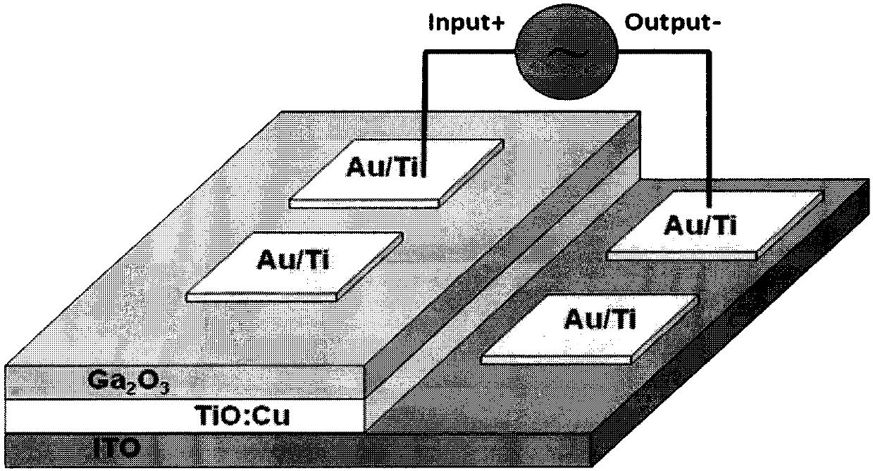
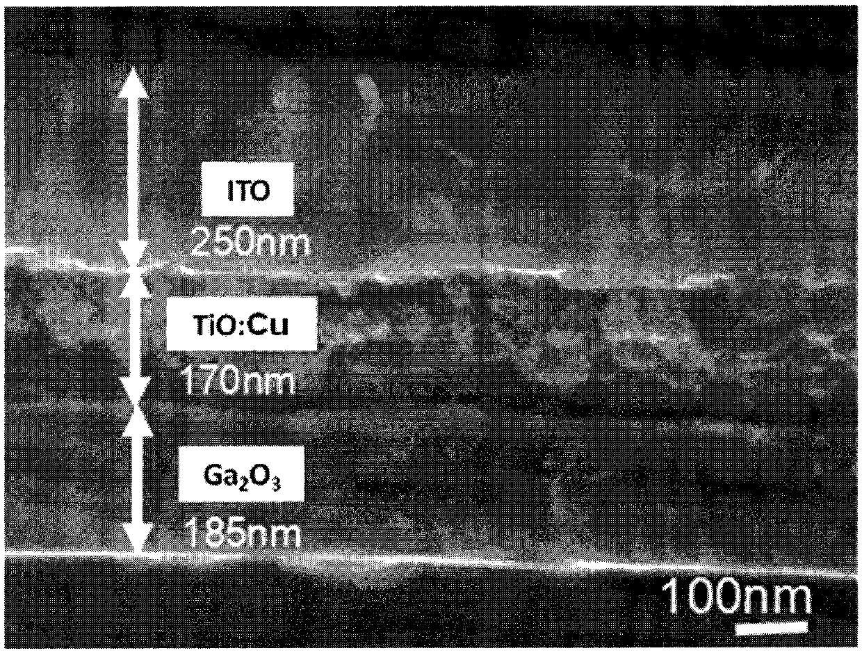
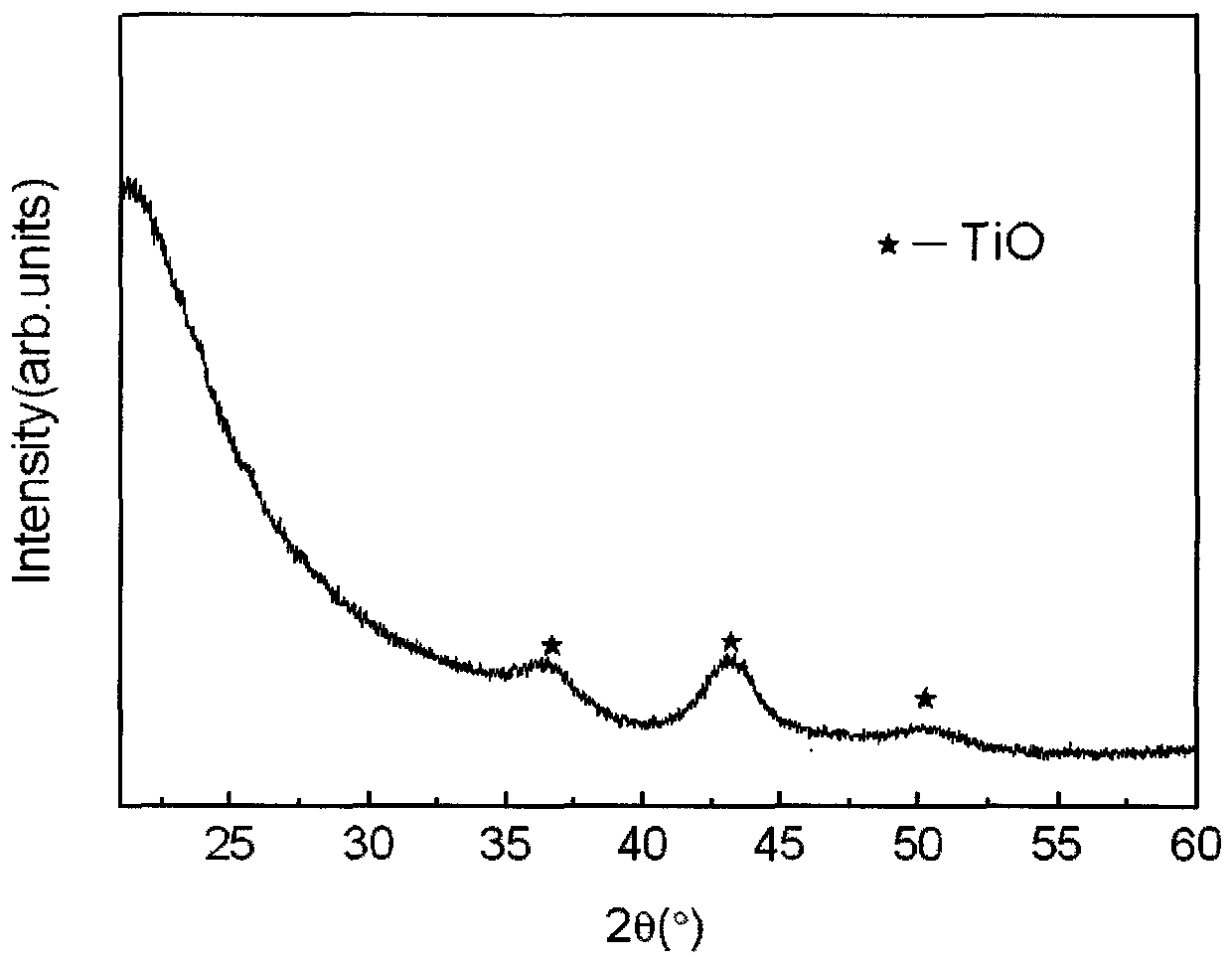
[0030] Take a piece of ITO substrate, ultrasonically clean it in deionized water, acetone, deionized water, ethanol, and deionized water for 5min, 15min, 5min, 15min, 5min, and dry naturally. The cleaned substrate was placed in the vacuum chamber of radio frequency magnetron sputtering, using Cu target (99.9%) and TiO 2 Target (99.9%) TiO:Cu films were deposited by co-sputtering with two targets. The chamber vacuum before sputtering is 1.6×10 -5 pa, the chamber pressure during sputtering is 1.0Pa, the argon gas flow in the chamber is 25sccm, the film deposition temperature is 300K at room temperature, the sputtering power of Cu target is 25W, TiO 2 The target sputtering power was 150W, and the total sputtering time was 1.0 hour. The resulting TiO:Cu film was vacuum annealed to a vacuum degree of 1.6×10 -5 pa, the annealing temperature is 573K, and the annealing time is ...


PUM

PropertyMeasurementUnit
thicknessaaaaaaaaaa
thicknessaaaaaaaaaa

Abstract

The invention discloses a multi-resistance state double-layer thin-film structure resistive variable memory and a preparation method thereof. The resistive variable memory has stable retention characteristics and multi-value storage performance. Specifically, it uses metal Ti / Au as the upper electrode, ITO as the substrate and the lower electrode, and uses radio frequency magnetron deposition technology to successively plate on the ITO substrate. TiO: Cu and Ga2O3 films to form a resistive layer, and then sputtering titanium (Ti) and gold (Au) films on the ITO substrate and the film that has been plated with gallium oxide to form ITO / TiO: Cu / Ga2O3 / Ti / Au structure memory device, and realize the multi-valued storage function. The advantage of the present invention is that single and bipolar resistive switching is generated through the movement of defects at the heterojunction interface, and the resistive switching memory device prepared has stable retention characteristics, cycle characteristics and multi-resistance state resistive switching storage performance, which improves the memory performance. storage capacity and service life.

Description

technical field [0001] The invention relates to a method for preparing a non-volatile resistive memory device, in particular to a resistive memory with a multi-resistance state double-layer film structure and a preparation method thereof. technical background [0002] Resistive RAM (RRAM) has the advantages of simple structure, high speed, low power consumption and easy 3D integration, and is an important new memory of the next generation. The principle of RRAM is that the resistance of the device changes reversibly between a low-resistance state (0) and a high-resistance state (1) under the action of an applied voltage, and the obtained resistance can be maintained after the external electric field is removed. In multi-value storage, more (for example, 0, 1, 2) stable states (that is, multiple resistance states in resistive memory) can be realized corresponding to different storage values. The application of multi-value storage technology can increase storage density, Incr...

Claims


Application Information

Patent Timeline
Patent Type & Authority Patents(China)
IPC IPC(8): H01L45/00H01L21/363
Inventor 金康康
Owner 江苏惠沣环保科技有限公司
Why Eureka
Try Eureka