Copper-fine-particle dispersion liquid, conductive-film formation method, and circuit board

A technology of copper particles and dispersions, applied to the formation of conductive patterns, conductive materials dispersed in non-conductive inorganic materials, conductive layers on insulating carriers, etc., can solve problems such as low resistance, failure to form, and insufficient photo-sintering , to achieve the effect of low resistance

Active Publication Date: 2015-12-30
ISHIHARA CHEM
View PDF8 Cites 0 Cited by
  • Summary
  • Abstract
  • Description
  • Claims
  • Application Information

AI Technical Summary

Problems solved by technology

[0004] However, even if the energy of the irradiated light used for photo-sintering in the above method is increased, photo-sintering may not proceed sufficiently, so that a conductive film having low resistance cannot be formed.

Method used


Image

  • Copper-fine-particle dispersion liquid, conductive-film formation method, and circuit board

Examples


Embodiment 1

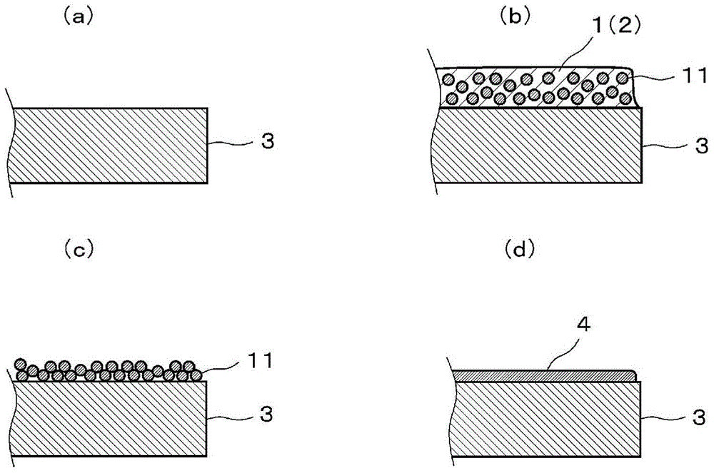
[0045] A copper particle dispersion is prepared in which a dispersant is added to disperse the copper particles in a dispersion medium. The dispersion medium is alcohol (diethylene glycol). This dispersion medium is also used as a sintering aid in this embodiment. The dispersant was phosphoric acid ester (trade name: "DISPERBYK (registered trademark)-102", available from BYK-Chemie). The concentration of the dispersant was 2% by mass relative to the copper fine particle dispersion. The copper fine particles used had an average particle size of 50 nm, and the concentration of the copper fine particles was 40% by mass. Glass slides were used as substrates.

[0046] The copper particle dispersion was applied to the substrate by spin coating to form a coating with a thickness of 1 μm. Coating color is black. The coating is irradiated with light without drying. Light irradiation energy is 14J / cm 2 .

[0047] The appearance of the coating changes to that of metallic copper b...

Embodiment 2

[0049] The dispersion medium used was an alcohol (diethylene glycol monoethyl ether) different from Example 1. This dispersion medium is also used as a sintering aid in this embodiment. Unlike Example 1, the dispersant used was a phosphoric acid ester (trade name: "DISPERBYK (registered trademark)-111", available from BYK-Chemie). Other conditions are identical with embodiment 1. The appearance of the coating changes to that of metallic copper by light irradiation, and a conductive film is formed on the substrate. The sheet resistance of the formed conductive film was 500 mΩ / sq.

Embodiment 3

[0051] Copper particle dispersions were prepared using copper particles having an average particle size of 70 nm. Then, phosphoric acid ester (trade name: "DISPERBYK (registered trademark)-111", available from BYK-Chemie) was added as a sintering aid to the copper particle dispersion. The sintering aid also acts as a dispersant. The concentration of the sintering aid was 10% by mass relative to the copper fine particle dispersion. A glass substrate (trade name "EAGLEXG (registered trademark)", available from Corning) was used as the substrate. Other conditions are identical with embodiment 2. A coating comprising a dispersion of copper particles is formed on a substrate. After the coating dries, the coating is irradiated with light. The energy of light irradiation is 11J / cm 2 . The appearance of the coating changes to that of metallic copper by light irradiation, and a conductive film is formed on the substrate. The sheet resistance of the formed conductive film was 170...


PUM

PropertyMeasurementUnit
thicknessaaaaaaaaaa
thicknessaaaaaaaaaa

Abstract

Provided is a copper-fine-particle dispersion liquid with which photosintering can be used to easily form a conductive film having a low electrical resistance. This copper-fine-particle dispersion liquid (1) includes a dispersion medium, and copper fine particles (11) dispersed in the dispersion medium. The copper-fine-particle dispersion liquid (1) includes a sintering promoter. The sintering promoter is a compound which removes copper oxide from copper at a temperature higher than room temperature. Accordingly, during photosintering of the copper fine particles (11), the sintering promoter removes a surface oxide film on the copper fine particles (11).

Description

technical field [0001] The present invention relates to a copper fine particle dispersion, a conductive film forming method using the copper fine particle dispersion, and a circuit board produced by using the conductive film forming method. Background technique [0002] Traditionally, printed circuit boards have formed copper foil circuits on the substrate by photolithography. Photolithography requires a step of etching copper foil, which incurs costs such as treating waste water generated by etching. [0003] As a technique that does not require etching, there is known a method of forming a conductive film (conductive membrane) (conductive film) on a base material using a copper fine particle dispersion (copper ink) containing copper in a dispersion medium. Copper microparticles (copper nanoparticles) (for example, see Patent Document 1). According to this method, a coating of a dispersion of copper particles is formed on a substrate, and the coating is dried to form a la...

Claims


Application Information

Patent Timeline
Patent Type & Authority Applications(China)
IPC IPC(8): H01B1/22B22F7/04B22F9/00C09D5/24C09D7/12H01B1/02H01B5/14H01B13/00H05K1/09H05K3/10
CPCB22F7/04C09D5/24H01B1/22H05K3/1216H05K3/125H05K3/1283H05K1/0386H05K2203/0508H05K2203/108H05K2203/1476H05K1/097C09D7/40H05K1/092H01B1/02C09D7/61B22F10/10Y02P10/25H05K3/10H05K3/105H05K2201/0302H05K2203/10H05K2203/1131
Inventor 川户祐一有村英俊工藤富雄
Owner ISHIHARA CHEM
Why Eureka
Try Eureka