Magnetic tunnel junction and preparation method thereof

A technology of magnetic tunnel junction and magnetic layer, applied in the field of magnetic tunnel junction and its preparation, can solve the problems of inability to take into account small device size, thermal stability compatibility, etc., and achieve shortened annealing time, low annealing temperature, and small size. high effect

Active Publication Date: 2016-01-27
HUAZHONG UNIV OF SCI & TECH
View PDF5 Cites 7 Cited by
  • Summary
  • Abstract
  • Description
  • Claims
  • Application Information

AI Technical Summary

Problems solved by technology

[0005] In view of the above defects or improvement needs of the prior art, the present invention provides a magnetic tunnel junction with perpendicular magnetic anisotropy, which can take into account the small size of the device, high thermal stability and compatibility with the CMOS process, thereby solving the problem of In the prior art, magnetic tunnel junction devices cannot simultaneously take into account the technical problems of small device size, thermal stability and compatibility with CMOS processes, so they can be widely used in sensors, storage devices and logic computing devices

Method used


Image

  • Magnetic tunnel junction and preparation method thereof
  • Magnetic tunnel junction and preparation method thereof
  • Magnetic tunnel junction and preparation method thereof

Examples


preparation example Construction

[0033] The preparation method of the above-mentioned magnetic tunnel junction comprises the following steps:

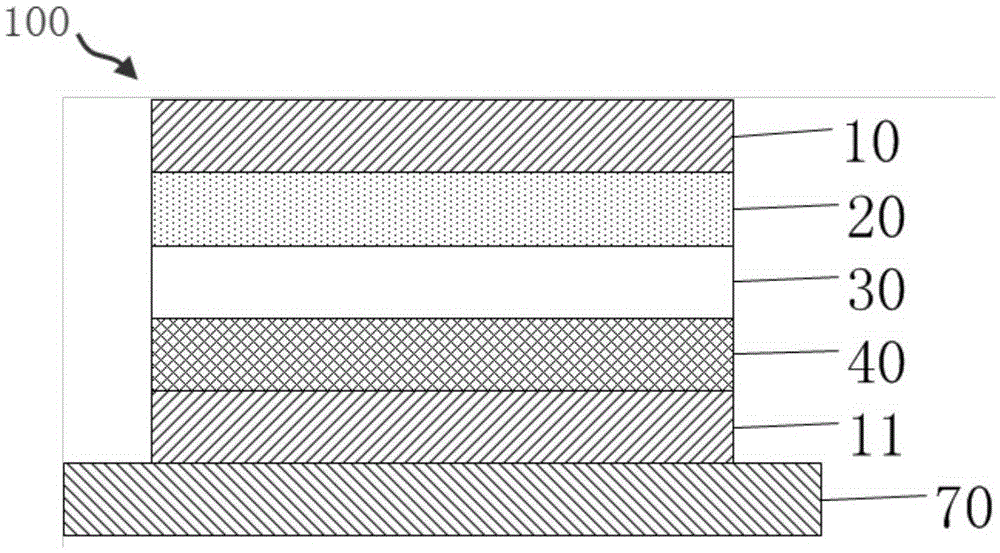
[0034] (1) depositing the first electrode material on the substrate 70, and patterning to obtain the first electrode layer 11;

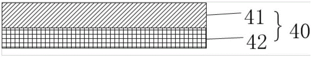
[0035] (2) sequentially depositing a first magnetic material, an insulating material and a second magnetic material on the first electrode layer 11, and patterning to obtain a first magnetic layer 40, an insulating tunneling layer 30 and a second magnetic layer 20;

[0036] (3) depositing a second electrode material on the second magnetic layer 20, and patterning to obtain the second electrode layer 10;

[0037] (4) Annealing at 300-500° C. for 5-10 minutes to obtain a magnetic tunnel junction.

[0038] Wherein, the first electrode material is obtained by sequentially depositing FePt and CoFe(R), and / or the second electrode material is obtained by sequentially depositing CoFe(R) and FePt, CoFe(R) is CoFe doped with R, R is B, At least one ...

Embodiment 1

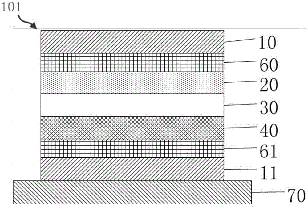
[0041] combine figure 1 , the preparation method of the above-mentioned magnetic tunnel junction comprises the following steps:

[0042] Step 101: providing a substrate 70, the substrate 70 is a thermally oxidized Si sheet or a CMOS chip;

[0043] Step 102: In an argon atmosphere, the first electrode layer 11 is prepared on the substrate 70 by magnetron sputtering, the deposition temperature is room temperature, the target material is Cu, and the vacuum degree is better than 10 -6 Pa, the thickness of the first electrode layer 11 is 200nm;

[0044] Step 103: In an argon atmosphere, the first magnetic layer 40 is prepared on the first electrode layer 11 by magnetron sputtering, which includes depositing a FePt layer on the first electrode layer 11 with a thickness of 3 nm, and then depositing CoFeB layer, the thickness is 5nm, the deposition temperature is room temperature, and the targets are Fe 50 Pt 50 alloy target and Co 40 Fe 40 B 20 target, the vacuum degree is bet...

Embodiment 2

[0052] The thickness of the FePt layer is 4.5nm, the thickness of the CoFeB layer is 5nm, and other steps are the same as in Embodiment 1.


PUM


Abstract

The invention discloses a magnetic tunnel junction and a preparation method thereof. The magnetic tunnel junction includes a first electrode layer, and a first magnetic layer, an insulation tunneling layer, a second magnetic layer, and a second electrode layer that are successively arranged on the first electrode layer, at least one of the first magnetic layer and the second magnetic layer is in a CoFe(R) / FePt structure, the CoFe(R) / FePt structure is formed by the overlapping of a CoFe(R) layer and a FePt layer, the CoFe(R) layer is closer to the insulation tunneling layer than the FePt layer, and the CoFe(R) layer is made of CoFe doped with R, and R is at least one of B, Al, and Ni. The magnetic tunnel junction concerns the compatibility of the small size of a device, the high thermal stability, and a CMOS process, so that the magnetic tunnel junction can be widely applied to a sensor, a storage device, and a logic calculating apparatus.

Description

technical field [0001] The invention belongs to the technical field of microelectronic devices, and more specifically relates to a magnetic tunnel junction and a preparation method thereof. Background technique [0002] When the material scale is equivalent to the physical characteristic length of conduction electrons, a series of magnetic materials with special properties appear, such as giant magnetoresistance materials, magnetic semiconductor materials, etc. In 1988, it was found in the magnetic metal multilayer film that its resistance changed by 50% under a magnetic field, so it was called the giant magnetoresistance effect (Giant MagnetoResistance, GMR). Based on this effect, the applied material—GMR spin valve was developed in the 1990s. Encouraged by GMR, in 1995 people realized a huge tunneling magnetoresistance effect (Tunnel MagnetoResistance, TMR) at room temperature in a magnetic tunnel junction. The basic structure of the magnetic tunnel junction is a sandwic...

Claims


Application Information

Patent Timeline
Patent Type & Authority Applications(China)
IPC IPC(8): H01L43/10H01L43/12
Inventor 程晓敏关夏威黄婷王升缪向水
Owner HUAZHONG UNIV OF SCI & TECH
Why Eureka
Try Eureka