Test structure and test method

A technology of test structure and test method, which is applied in the direction of semiconductor/solid-state device test/measurement, single semiconductor device test, electrical components, etc. Problems such as failure location to achieve good test results

Active Publication Date: 2016-02-03
SEMICON MFG INT (SHANGHAI) CORP
View PDF4 Cites 12 Cited by
  • Summary
  • Abstract
  • Description
  • Claims
  • Application Information

AI Technical Summary

Problems solved by technology

[0006] In view of the shortcomings of the prior art described above, the purpose of the present invention is to provide a test structure and a test method for solving the problem that there is no effective me

Method used


Image

  • Test structure and test method
  • Test structure and test method
  • Test structure and test method

Examples


Embodiment 1

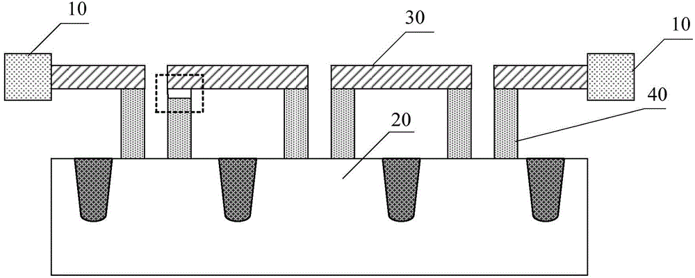
[0038] see image 3 , the present invention provides a test structure, the test structure can be designed on the wafer dicing road, including a substrate layer 1 and a number of discrete first interlayer metal layers 2, the first interlayer metal layer 2 and the The substrate layers 1 are electrically connected through a number of first contact plugs 3; the test structure also includes a second interlayer metal layer 4 distributed continuously, and the second interlayer metal layer 4 is connected through a number of second contact plugs. It is electrically connected with the first interlayer metal layer 2 described in 5 .

[0039] Specifically, the substrate layer 1 may be a device layer or a metal interconnection layer. That is, the test structure of the present invention can be used to monitor the contact condition between the contact layer (CT layer) and the first metal layer (metal-1) on the device layer, and can also be used to monitor a certain via layer ( Via layer) a...

Embodiment 2

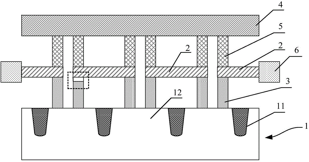
[0046] The present invention also provides a test method for testing the top contact of a contact plug using the test structure in Embodiment 1, which at least includes the following steps: firstly remove the substrate layer 1 from the back of the test structure to expose the first contact plugs 3, and then observe the lightness and darkness of the first contact plugs under a scanning electron microscope, if one of the first contact plugs is darker than the other first contact plugs, then it is judged that the first contact plug is different from the other first contact plugs. The disconnected connection between the first interlayer metal layers.

[0047] see Figure 4 , is shown as a cross-sectional view of the test structure after the substrate layer has been removed. At this time, observing the lightness and darkness of the first contact plug 3 under a scanning electron microscope can locate the disconnected connection position.

[0048] Specifically, the substrate layer ...


PUM


Abstract

The invention provides a test structure. The test structure comprises a substrate layer and a plurality of discrete first inter-layer metal layers, wherein the first inter-layer metal layers are in electrical connection with a plurality of first contact plugs; and the test structure further comprises a continuously distributed second inter-layer metal layer, wherein the second inter-layer metal layer is in electrical connection with the first inter-layer metal layers through a plurality of second contact plugs. According to the invention, the first inter-layer metal layers are connected to a big second inter-layer metal layer through the second contact plugs, thus, the effect of grounding is realized, and potential difference of the surface of the first contact plugs after the metal is in broken line connection is enhanced; and based on the principle of voltage contrast of a scanning electron microscope, light and shade degree of the first contact plugs can be observed from the back of a wafer so as to reflect whether the first contact plugs are contacted well with the first inter-layer metal layers, thus, locations of defect can be found quickly, process defects can be reflected, and the aim of early defect monitoring is realized.

Description

technical field [0001] The invention belongs to the field of semiconductor manufacturing, and relates to a test structure and a test method. Background technique [0002] As the density of chip devices increases, the size of metal wiring becomes smaller and smaller, and the aspect ratio of metal etching becomes larger and larger. Underetch of the metal layer is prone to occur, resulting in yield loss. [0003] During the semiconductor chip manufacturing process or when the manufacturing is completed, it is necessary to test the parameters related to the semiconductor chip to monitor whether the produced semiconductor chip meets the process requirements and whether the yield rate is qualified, etc. The test of the relevant parameters is usually through setting and cutting. It is done by the test structure (TestKey) of the channel area. In the test structure design, there will be a contact chain (CTchain) on the chip to monitor the connection between CT (contact, contact) and...

Claims


Application Information

Patent Timeline
IPC IPC(8): H01L23/544H01L21/66G01R31/26
Inventor 杨梅
Owner SEMICON MFG INT (SHANGHAI) CORP
Why Eureka
Try Eureka