MEMS sandwich accelerometer sensitive chip wet etching processing method

A wet corrosion and accelerometer technology, which is used in the measurement of acceleration, velocity/acceleration/impact measurement, acceleration measurement using inertial force, etc., to achieve the effect of simple process, high reliability, and improved corrosion processing quality

Inactive Publication Date: 2016-02-17
BEIJING INST OF AEROSPACE CONTROL DEVICES
View PDF5 Cites 3 Cited by
  • Summary
  • Abstract
  • Description
  • Claims
  • Application Information

AI Technical Summary

Problems solved by technology

[0007] The technical problem to be solved by the present invention is: to overcome the deficiencies in the prior art, and provide a wet etching

Method used


Image

  • MEMS sandwich accelerometer sensitive chip wet etching processing method
  • MEMS sandwich accelerometer sensitive chip wet etching processing method
  • MEMS sandwich accelerometer sensitive chip wet etching processing method

Examples


Example Embodiment

[0028] The detailed process of the present invention is introduced in detail below:

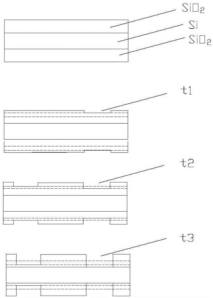
[0029] 1) To generate silicon wafer oxide film, perform wet oxygen oxidation on silicon wafer at 1000-1100°C, oxygen flow rate is 0.6-1.0l / min, oxidation time is more than 20 hours, and film thickness is 3μm-3.2μm at t;

[0030] The chemical reaction formula for the formation of wet oxide layer is:

[0031] Si+2H 2 O = SiO 2 +2H 2

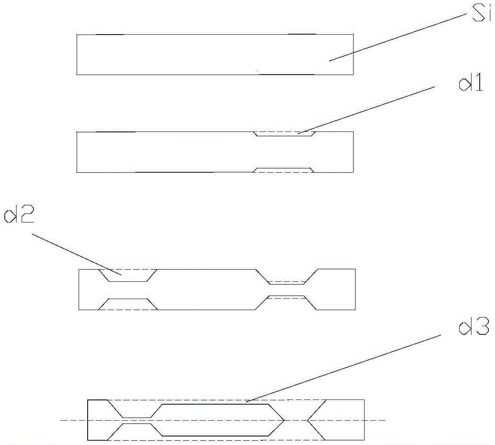
[0032] 2) Three times of layered processing on the oxide film, three times of conventional double-sided photolithography etching on the oxide film, the structure is formed by transferring three different positive resist patterns, and the pattern part of each exposure includes For the graphic part of the last exposure, the processing and etching size is below 3 microns. During photolithography, the surface of the oxide film of the silicon wafer can be treated as a relatively flat plane, and it is etched under the protection of glue every time. The etching solut...


PUM


Abstract

The present invention discloses a MEMS sandwich accelerometer sensitive chip wet etching processing method, a single-layer oxide layer is grown on a silicon wafer, double-sided lithographic etching the single-layer oxide film layer is performed for 3 times, the depth of each tie of etching is precisely controlled, and the single-layer oxide film layer is divided into three layers of different structures of oxide film layers. At a temperature of 60-80 DEG C, the silicon wafer is wet-etched, the first silicon etching time is 20 to 30 minutes, the first layer oxide film layer is etched; the second silicon etching time is 150 to 160 minutes, the second layer oxide film layer is etched; the silicon wafer is wet-etched at a temperature of 30-40 DEG C in the third etching, the etching time is 30 to 40 minutes, and the third layer oxide film layer is etched. A sensitive chip with smooth surface and accurate dimension can be processed by the method, and by improvement of the method, the quality and rate of finished products of the sensitive chip can be greatly improved.

Description

technical field [0001] The invention relates to the field of micro-electro-mechanical system processing, in particular to a wet-etching processing method for sensitive chips of MEMS sandwich accelerometers. Background technique [0002] MEMS accelerometers have been widely used in many fields such as national defense, inertial navigation, earthquake detection, industry, medical treatment, automation, and consumer electronics due to their low cost, small size, low power consumption, and mass production. [0003] The MEMS sandwich accelerometer is manufactured by bulk micromachining technology, and the process is relatively complicated but it is easier to obtain high detection accuracy. The sensitive chip is a key component of the MEMS sandwich accelerometer, and its corrosion process is the most critical. [0004] The silicon etching process is divided into dry etching and wet etching. [0005] Dry etching is the use of gas molecules under the action of a strong electric fi...

Claims


Application Information

Patent Timeline
IPC IPC(8): B81C1/00G01P15/08
CPCB81C1/00539G01P15/0802
Inventor 刘宇刘福民邢朝洋徐宇新李昌政刘国文梁德春
Owner BEIJING INST OF AEROSPACE CONTROL DEVICES
Why Eureka
Try Eureka