High performance MTJ element for STT-RAM and method for making the same

a sttram and high-performance technology, applied in the direction of inductance/transformer/magnet manufacture, magnetic bodies, instruments, etc., can solve the problems of introducing statistical difficulties, and affecting the effect of sttram performan

Active Publication Date: 2010-07-06
TAIWAN SEMICON MFG CO LTD
View PDF14 Cites 96 Cited by
  • Summary
  • Abstract
  • Description
  • Claims
  • Application Information

AI Technical Summary

Benefits of technology

[0044]A second object of this invention is to provide a MTJ element for an STT-RAM configured MRAM device in which the intrinsic (unbiased) and operational (biased) TMR ratio, dR / R, is significantly enhanced and wherein the intrinsic dR / R is between about 125% to 130%.
[0048]A sixth object of the present invention is to provide such an MTJ element wherein the structure of the pinning / pinned layer provides a low angular dispersion of the pinned layer magnetic moment direction, preferably 1.6× less than that of conventional configurations.
[0049]These objects will be met by an MTJ element structure in which the free layer damping constant (Gilbert damping constant α) is reduced to less than that associated with only a free layer of amorphous CoFeB, in which the tunnel barrier layer is deposited in a crystalline form by means of being sputtered from an Mg target and then naturally oxidized, in which highly efficient and enhanced spin polarization is obtained by surrounding the free layer by layers of crystalline Fe and in which the antiferromagnetic pinning layer is a layer of MnIr.
[0051]Buffer layer / Pinning layer / / Co75Fe2523 / Ru7.5 / Co60Fe20B2015-CO 75Fe25(API) / Mg8-NOX—Mg4 / Fee layer / Ta30RuWhere the general ordering of the layers is as in FIG. 2. In the preferred embodiment, the free layer is of the form Fe 3 / CoFeB 20 / Fe 6, with the two interfacial Fe layers being very thin (respectively 3 and 6 angstroms) and crystalline in structure for enhanced spin polarization of the current, while the CoFeB layer sandwiched between them is amorphous in form to obtain a low Gilbert magnetic damping factor. The tunneling barrier layer is a layer of MgO that is rendered crystalline in nature by being formed by a combination of a sputtering deposition of Mg and a natural oxidation process. The sputtering is onto an exposed surface of AP1 that has been preconditioned by a plasma treatment to render it smooth / flat. This plasma pretreatment is, in turn, highly advantageous, given the fact that the pinning layer for the SyAF pinned layer is a layer of MnIr rather than the more usual MnPt. The MnIr pinning layer, in turn, allows an advantageous annealing process in which the anneal need only be carried out at 265° C. for between 1 and 2 hours in a magnetic field of 10 K Oe. It is to be noted that other prior art processes form the MgO tunneling barrier layer by sputtering directly from an MgO target. This produces an amorphous layer which must be rendered crystalline by use of much higher annealing temperatures than are required in the present invention.

Problems solved by technology

Needless to say, this process also introduces some statistical difficulties associated with the variation of resistances of the cells.
The use of magnetic fields externally generated by current carrying lines (as in FIG. 1) to switch the magnetic moment directions becomes problematic as the size of the MRAM cells decreases and, along with their decrease, so must the width of the current carrying lines.
The smaller width lines require greater currents to produce the necessary switching fields, greatly increasing power consumption.
This high current density, which is required to induce the spin transfer effect, could destroy the insulating tunneling barrier in the MTJ cell, such as a layer of AlOx, MgO, etc.
If the active device resistances in a block of memory show a high variation in resistance (i.e. high Rp covariance, or Rap covariance), a signal error can occur when they are compared with the reference cell.
This value would not be sufficient to provide a good read margin.

Method used


Image

  • High performance MTJ element for STT-RAM and method for making the same
  • High performance MTJ element for STT-RAM and method for making the same
  • High performance MTJ element for STT-RAM and method for making the same

Examples


Embodiment Construction

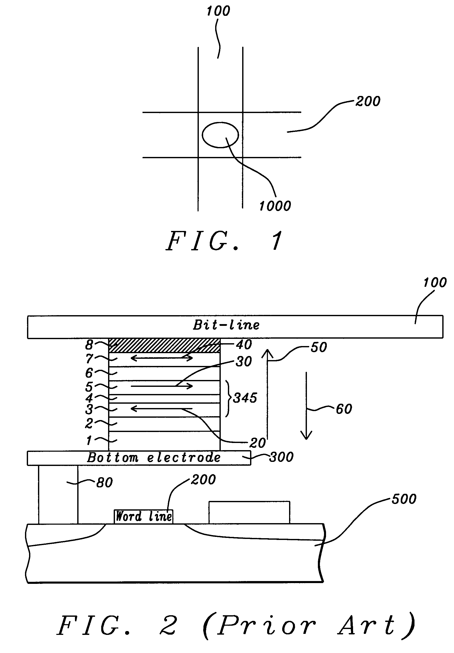
[0059]The preferred embodiment of the present invention is an STT-RAM memory cell and an array of such cells, in which each cell incorporates an MTJ element that operates in the spin torque transfer (STT) mode. The MTJ element includes an IrMn pinning layer, an SyAP pinned layer, a crystalline barrier layer of naturally oxidized MgO and a crystalline-Fe-sandwiched CoFeB free layer having Gilbert damping constants that are lower than those associated with free layers of only amorphous CoFeB.

[0060]The preferred MTJ stack configuration is:[0061]BE / NiCr50 / Ru20 / MnIr70 / Co75Fe2523 (AP2) / Ru7.5 / CoFeB20—Co75Fe256-7 (AP1) / PT / Mg8-NOX—Mg4 / Fe3-Co60Fe20B2020-Fe6(FL) / Ta

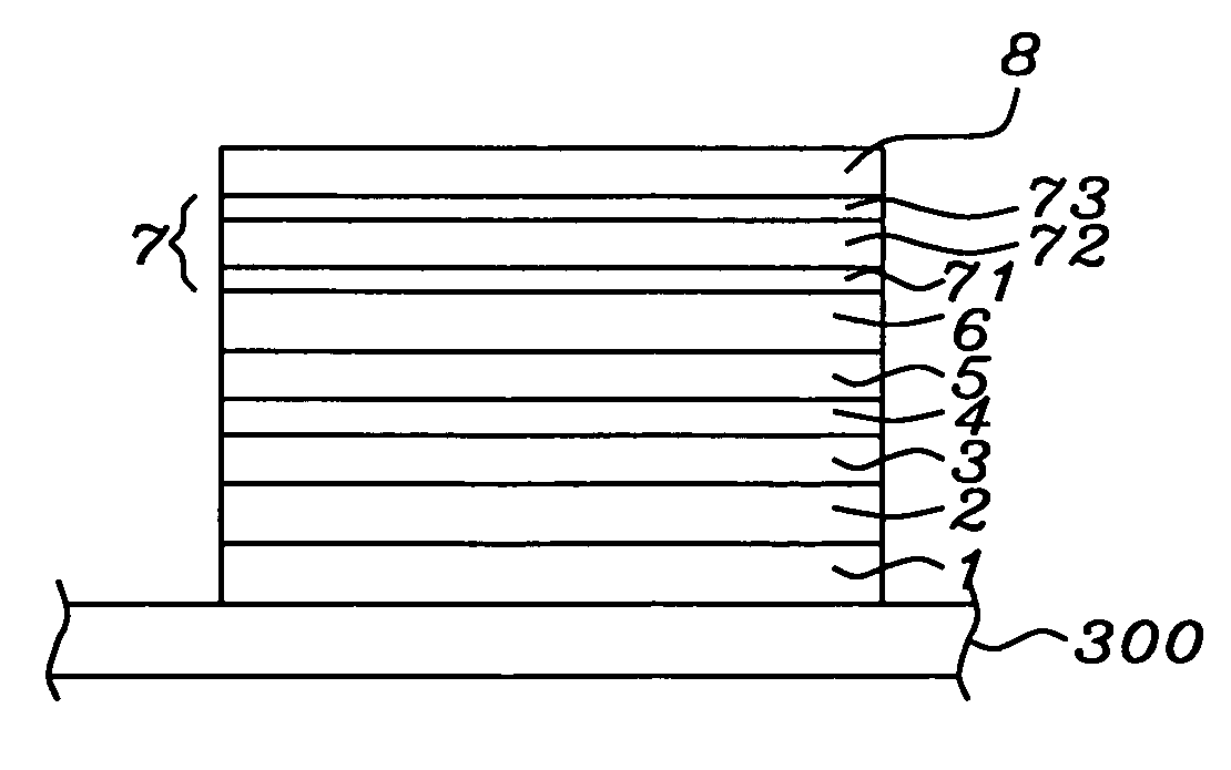
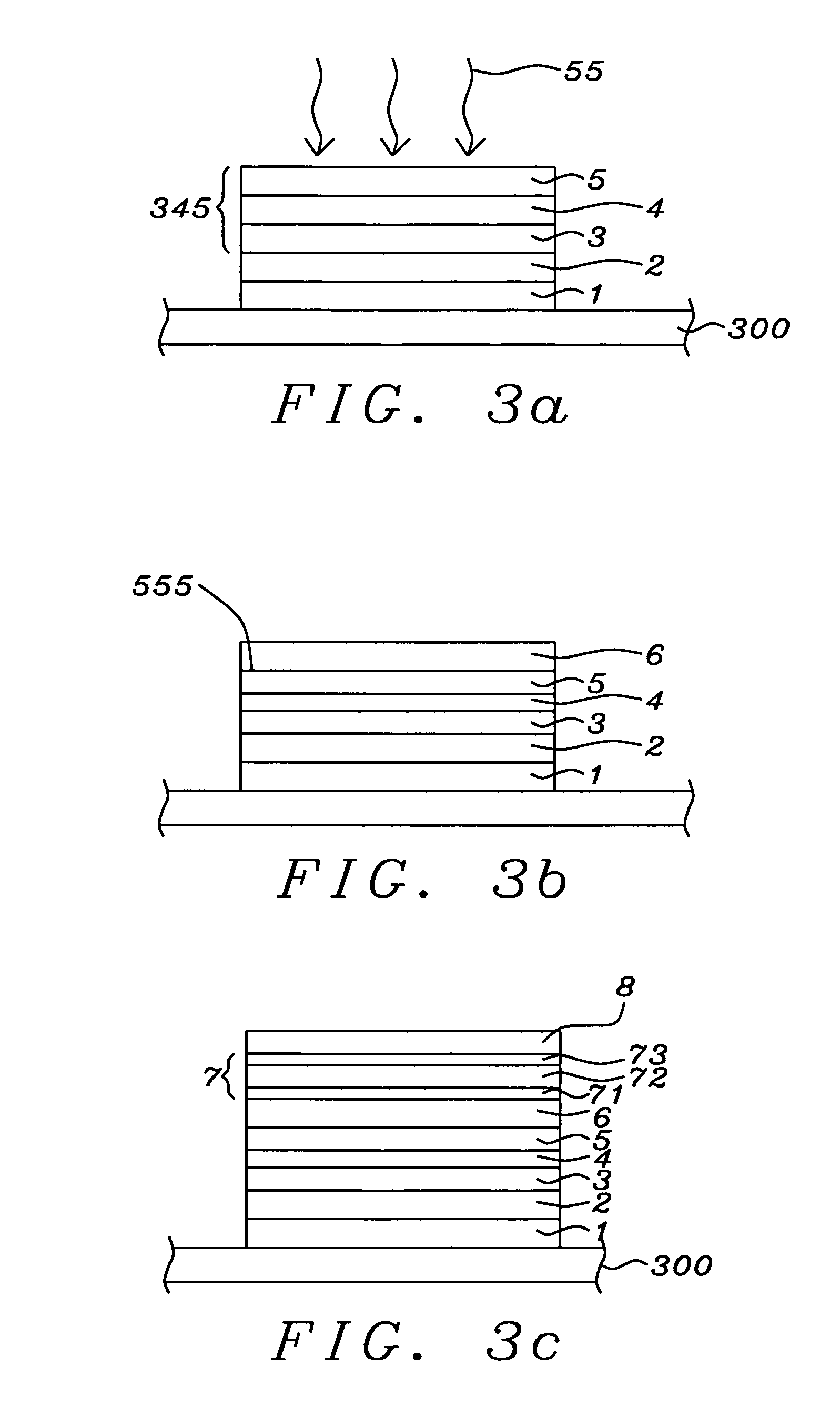
[0062]Referring to FIG. 3a, FIGS. 3b and 3c, there will be schematically shown the process steps by which the stack configuration is formed. We will retain the essential elements of the numbering of FIG. 2.

[0063]Referring first to FIG. 3a, there is shown the structure labeled BE above, which denotes a bottom conducting line or electr...


PUM


Abstract

A STT-MTJ MRAM cell that utilizes transfer of spin angular momentum as a mechanism for changing the magnetic moment direction of a free layer includes an IrMn pinning layer, a SyAP pinned layer, a naturally oxidized, crystalline MgO tunneling barrier layer that is formed on an Ar-ion plasma smoothed surface of the pinned layer and, in one embodiment, a free layer that comprises an amorphous layer of Co60Fe20B20 of approximately 20 angstroms thickness formed between two crystalline layers of Fe of 3 and 6 angstroms thickness respectively or on a single such layer. The free layer is characterized by a low Gilbert damping factor and by very strong polarizing action on conduction electrons. The resulting cell has a low critical current, a high dR / R and a plurality of such cells will exhibit a low variation of both resistance and pinned layer magnetization angular dispersion.

Description

BACKGROUND OF THE INVENTION[0001]1. Field of the Invention[0002]This invention relates generally to a current perpendicular to plane (CPP) magnetic random access memory (CPP-MRAM) cell formed using a magnetic tunneling junction (MTJ) as the basic memory element, wherein a spin torque transfer (STT) effect is used to change the magnetization direction of the MTJ ferromagnetic free layer.[0003]2. Description of the Related Art[0004]The conventional magnetic tunneling junction (MTJ) device is a form of ultra-high magnetoresistive device in which the relative orientation of the magnetic moments of parallel, vertically separated, upper and lower magnetized layers controls the flow of spin-polarized electrons tunneling through a very thin dielectric layer (the tunneling barrier layer) formed between those layers. When injected electrons pass through the upper layer they are spin polarized by interaction with the magnetic moment of that layer. The majority of the electrons emerge polarized...

Claims


Application Information

Patent Timeline
Patent Type & Authority Patents(United States)
IPC IPC(8): H01L29/82
CPCB82Y25/00B82Y40/00G11C11/16H01F10/3272H01F10/329H01F41/307H01L43/08H01L43/10H01L43/12H01F10/3295G11C11/161H10N50/85H10N50/01H10N50/10
Inventor HORNG, CHENG T.TONG, RU-YINGTORNG, CHYU-JIUHKULA, WITOLD
Owner TAIWAN SEMICON MFG CO LTD
Why Eureka
Try Eureka