

A control device for atomic layer deposition instrument
A technology for controlling equipment and deposition apparatus, applied in the field of atomic layer deposition control, can solve the problems that have not yet been developed, and achieve the effects of easy equipment maintenance, low production cost and powerful functions
- Summary
- Abstract
- Description
- Claims
- Application Information
AI Technical Summary
Problems solved by technology
Method used
Image

Examples
example 1
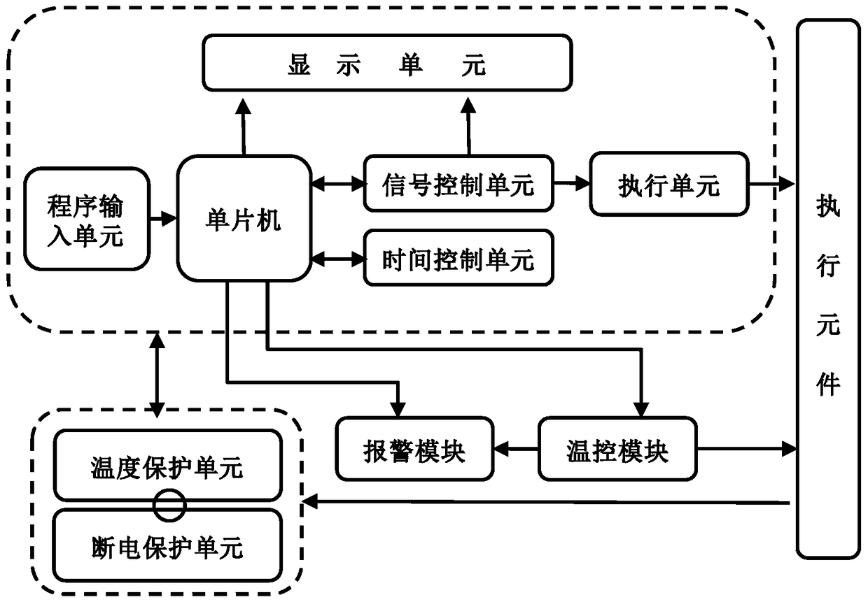
[0052] Example 1. Such as Figure 7 As shown, a typical atomic layer deposition program flow is set as follows: the system contains 2 high-speed valves, 1 baffle valve, 5 heating channels and a pressure detector, and the program can control different set temperatures of the heating channels (from room temperature to to 300 degrees Celsius), flapper valve closing and waiting time, high-speed valve opening time. The flow of the program can set the pumping times of the precursors (n1 and n1’) respectively, set the total reaction cycle times (m1), and keep monitoring the pressure of the system.
example 2
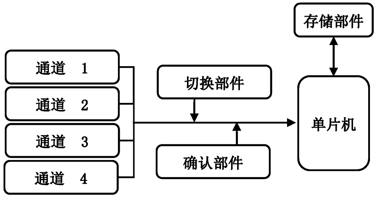
[0053] Example 2. Set the control signals of the three channels of the field effect transistor (MOS transistor) execution unit through the microcontroller (such as Figure 8 As shown), each channel can control a gas path of a reaction precursor. For example, starting from 0 seconds, channel 1 sends out a pulse of 10 milliseconds every 10 seconds; starting from the third second, channel 2 sends out a pulse of 10 milliseconds every 10 seconds, and starting from the sixth second, channel 3 sends out a pulse of 10 milliseconds every 10 seconds The pulse voltage (such as 24 volts) can open the ALD high-speed valve to pump in the reaction precursor. After the pulse ends, the ALD high-speed valve is closed to stop pumping in the reaction precursor.
example 3
[0054] Example 3. Modulate the time when the baffle valve is opened, the baffle valve of the atomic layer deposition instrument is controlled by a single-chip computer to close d1 (such as 24) seconds, open d2 (such as 38) seconds, cycle operation, and keep nitrogen in the reactor during the same flow rate at 20 ml / sec. When the flapper valve is closed, the pressure of the system gradually rises, the closing time is 24 seconds, and the pressure rises to a very high value; when the flapper valve is opened, the residual gas in the system is sucked away by the vacuum system, the system pressure drops, and the opening time is 38 seconds , the pressure tends to be stable; when the cycle is in progress, the pressure of the system changes periodically (such as Figure 9 shown).
PUM
 Abstract
Description
Claims
Application Information