Preparation method of silk fiber-based patterned semiconductor polymer film

A technology of polymer film and silk fiber, applied in the field of polymer patterning preparation, can solve the problems of soft template preparation process conditions, soft template easily affected by organic solvents, complicated hard template preparation process, etc. The effect of reducing the difficulty of preparation, low cost and reducing preparation cost

Active Publication Date: 2016-02-24
HUAIBEI NORMAL UNIVERSITY
View PDF4 Cites 4 Cited by
  • Summary
  • Abstract
  • Description
  • Claims
  • Application Information

AI Technical Summary

Problems solved by technology

Hard templates have high structural dimensional stability and fidelity when constructing nano-patterns, but the preparation process of hard templates is complicated, the overall cost of preparation is expensive, and the operating conditions are relatively harsh in the process of constructing micro-nano patterns. irreversible template damage
In order to make up for the shortage of hard templates, soft template technology emerged as the times require. Soft templates are not prone to irreversible damage during the process of pattern preparation, but the dimensional stability of the pattern structure of soft templates and the process conditions for pattern preparation have also become problems. For example, soft templates are easy to Affected by organic solvents, the rigidity of the soft template is still very limited, etc.

Method used


Image

  • Preparation method of silk fiber-based patterned semiconductor polymer film
  • Preparation method of silk fiber-based patterned semiconductor polymer film
  • Preparation method of silk fiber-based patterned semiconductor polymer film

Examples


Embodiment 1

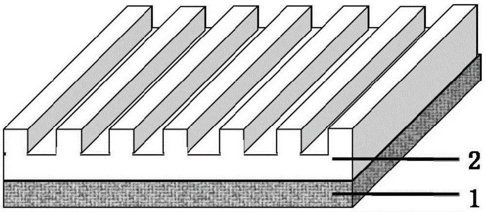
[0033] ①Using the existing electron beam exposure technology to process the surface of the photoresist film to prepare the micro-nano pattern of the line structure, the characteristic structure size is 250 nanometers, in figure 1 Among them, 1 represents the silicon substrate S1 which only serves as a substrate support, and 2 represents the photoresist PMMA (an existing commercially available product).

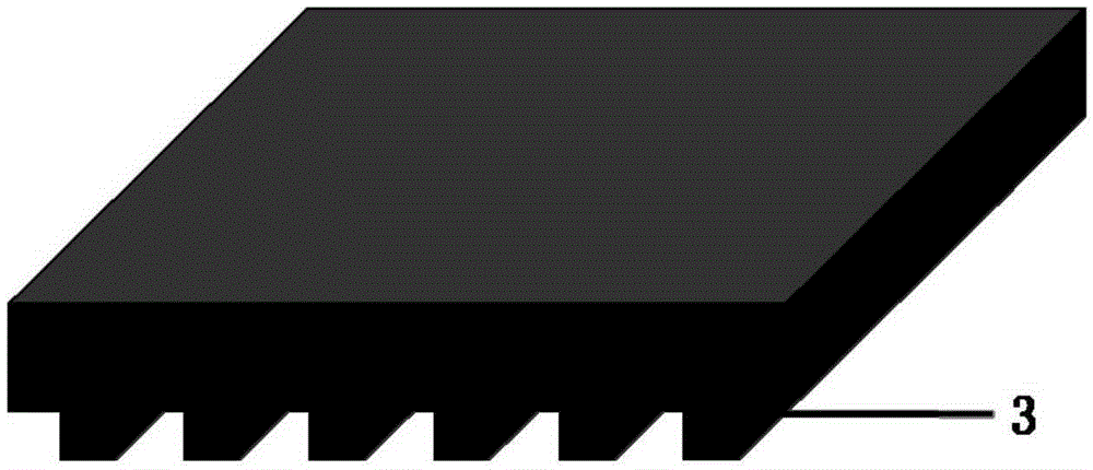
[0034] ② Evenly coat the uncrosslinked PDMS solution (commercially available product) on the surface of the photoresist film with micro-nano structure, place the whole in a vacuum drying oven, and conduct heating and crosslinking. The crosslinking conditions are: vacuum degree 0.09 MPa, the heating temperature is 65 degrees Celsius, and the crosslinking time is 30 minutes; after crosslinking, the PDMS soft template is uniformly removed from the surface of the photoresist, so that the surface of the PDMS soft template has a micro-nano structure complementary to the pattern struc...

Embodiment 2

[0039] ①Using electron beam exposure technology to prepare micro-nano pattern of line structure on the surface of photoresist film, the characteristic structure size is 200 nanometers, in figure 1 Among them, 1 represents the silicon substrate S1 which only serves as a substrate support, and 2 represents the photoresist PMMA.

[0040] ② Evenly coat the uncrosslinked PDMS solution on the surface of the photoresist film with micro-nano structure, place the whole in a vacuum drying oven, and heat and crosslink. After the sufficient crosslinking treatment is completed, the PDMS soft template It is uniformly removed from the surface of the photoresist, so that the surface of the PDMS soft template has a complementary micro-nano structure pattern on the surface of the photoresist, such as figure 2 As shown, 3 represents the PDMS organic material.

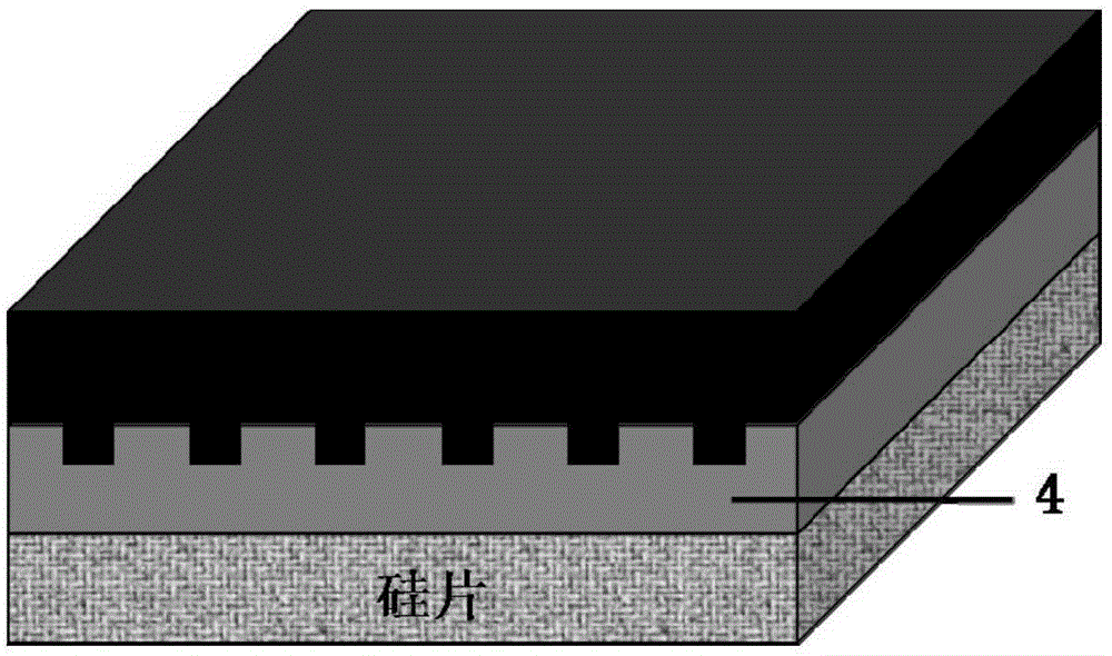
[0041] ③ Preparation of silk fiber aqueous solution: put natural silk into 0.06% sodium carbonate aqueous solution, degumming treatmen...


PUM

PropertyMeasurementUnit
Thicknessaaaaaaaaaa
Thicknessaaaaaaaaaa

Abstract

The invention discloses a preparation method of a silk fiber-based patterned semiconductor polymer film. The method is mainly used for preparing a micro-nano pattern of a semiconductor polymer film material. The method comprises the following steps: firstly, preparing a required complementary size of the micro-nano pattern of a semiconductor polymer film on the surface of a photoresist film by an exposure technology; secondly, coating the surface of the photoresist film with the pattern with an uncrosslinked PDMS material, carrying out a thermal crosslinking treatment, taking down a soft template formed by the PDMS and making a photoresist pattern transferred to the surface of the soft template of a PDMS film; thirdly, putting the PDMS film with the micro-nano pattern on a silk fiber water solution, and preparing the silk fiber film with a micro-nano structure after room-temperature drying treatment; and finally, with the silk fiber film as the template, achieving patterning of different semiconductor polymer films by nanoimprint lithography. The preparation method has the advantages of simplicity in step, low cost, large area, low requirements on operation conditions and the like, is especially applicable to organic semiconductor materials which are high in rigidity or are patterned at a room temperature, and has a good practical application value.

Description

technical field [0001] The invention discloses a method for preparing a patterned polymer, in particular to a method for preparing a patterned semiconductor polymer film based on silk fibers. Background technique [0002] Since the discovery of semiconducting polymers, due to their special electrical and optical properties, coupled with a series of advantages such as lightness, transparency, easy processing and low cost of polymers, research on conductive polymers has become more and more popular. people's attention. With the continuous demand for miniaturization and low cost of organic semiconductor devices, the development of organic semiconductor devices has become increasingly inseparable from the patterning of semiconducting polymer materials. For example, in organic light emitting diode (OLED) technology, it is necessary to integrate three primary color light-emitting materials into one pixel, and the size of each pixel has been developed from micron to nanometer. ...

Claims


Application Information

Patent Timeline
IPC IPC(8): H01L21/027G03F7/20
CPCG03F7/20H01L21/027
Inventor 丁光柱刘结平胡志军
Owner HUAIBEI NORMAL UNIVERSITY
Why Eureka
Try Eureka