A light-emitting diode epitaxial wafer and its manufacturing method

A technology of light-emitting diodes and manufacturing methods, which is applied in semiconductor/solid-state device manufacturing, gaseous chemical plating, coating, etc., can solve the problems of low luminous efficiency of LEDs, improve luminous efficiency, increase the number of holes, and facilitate diffusion Effect

Active Publication Date: 2018-08-03
HC SEMITEK CORP
View PDF3 Cites 0 Cited by
  • Summary
  • Abstract
  • Description
  • Claims
  • Application Information

AI Technical Summary

Problems solved by technology

[0006] In order to solve the problem of low luminous efficiency of LEDs in the prior art, an embodiment o

Method used


Image

  • A light-emitting diode epitaxial wafer and its manufacturing method
  • A light-emitting diode epitaxial wafer and its manufacturing method

Examples


Embodiment 1

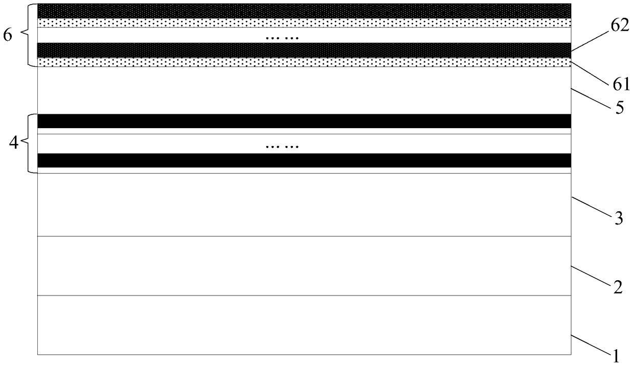
[0028] An embodiment of the present invention provides a light emitting diode epitaxial wafer, see figure 1 The light-emitting diode epitaxial wafer includes a substrate 1, and an undoped GaN layer 2, an N-type GaN layer 3, a multiple quantum well layer 4, a P-type AlGaN electron blocking layer 5, and a P-type layer stacked on the substrate 1 in sequence. 6.

[0029] In this embodiment, the multiple quantum well layer 4 includes alternately grown InGaN layers and GaN layers. The P-type layer 6 includes alternately grown P-type GaN layers 61 and undoped GaN layers 62 .

[0030] Optionally, the thickness of the undoped GaN layer 62 in the P-type layer 6 may be 2-3 nm. When the thickness of the undoped GaN layer 62 in the P-type layer 6 was less than 2nm, the undoped GaN layer 62 in the P-type layer 6 would not be able to form a continuous film because it was too thin, and the formed P-type layer 6 The quality of the undoped GaN layer 62 is poor; when the thickness of the undo...

Embodiment 2

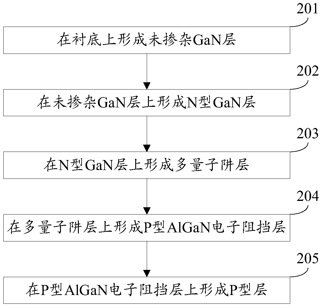
[0036] An embodiment of the present invention provides a method for manufacturing a light-emitting diode epitaxial wafer, see figure 2 , the production method includes:

[0037] Step 201: forming an undoped GaN layer on a substrate.

[0038] Step 202: forming an N-type GaN layer on the undoped GaN layer.

[0039] Step 203: forming a multi-quantum well layer on the N-type GaN layer.

[0040] In this embodiment, the multiple quantum well layer includes alternately grown InGaN layers and GaN layers.

[0041] Step 204: forming a P-type AlGaN electron blocking layer on the multi-quantum well layer.

[0042] Step 205: forming a P-type layer on the P-type AlGaN electron blocking layer.

[0043] In this embodiment, the P-type layer includes alternately grown P-type GaN layers and undoped GaN layers.

[0044] Optionally, the thickness of the undoped GaN layer in the P-type layer may be 2-3 nm. When the thickness of the undoped GaN layer in the P-type layer is less than 2nm, the ...


PUM

PropertyMeasurementUnit
Thicknessaaaaaaaaaa
Thicknessaaaaaaaaaa
Thicknessaaaaaaaaaa

Abstract

The invention discloses a light-emitting diode epitaxial wafer and a manufacturing method thereof, belonging to the technical field of semiconductors. The light-emitting diode epitaxial wafer includes a substrate, and an undoped GaN layer, an N-type GaN layer, a multi-quantum well layer, a P-type AlGaN electron blocking layer, and a P-type layer sequentially stacked on the substrate. The P-type layer includes alternately grown P-type GaN layers and undoped GaN layers. The present invention forms a P-type layer by alternately growing P-type GaN layers and undoped GaN layers, and the undoped GaN layer in the P-type layer has an accumulation effect on holes, so the hole concentration in the P-type GaN layer can be increased, Moreover, the undoped GaN layer in the P-type layer will not be affected by the scattering of unionized Mg, which is beneficial to the diffusion of holes, and also increases the migration efficiency of holes, thereby increasing the number of holes recombined with electrons in the multi-quantum well layer. The number of holes increases the luminous efficiency of the LED.

Description

technical field [0001] The invention relates to the technical field of semiconductors, in particular to a light-emitting diode epitaxial wafer and a manufacturing method thereof. Background technique [0002] Gallium nitride (GaN) is a typical representative of the third-generation wide-bandgap semiconductor materials. Its excellent physical and chemical properties make it have great application prospects in the fields of microelectronic devices and optoelectronic devices. GaN-based light-emitting diodes (Light Emitting Diode, referred to as LED) have the characteristics of small size, high brightness, and low energy consumption, and are widely used in the fields of display screens, backlight sources, and lighting. [0003] Epitaxial wafers are an important part of making LEDs. The existing light-emitting diode epitaxial wafer includes a substrate, and an undoped GaN layer, an N-type GaN layer, a multi-quantum well layer, a P-type AlGaN electron blocking layer and a P-type ...

Claims


Application Information

Patent Timeline
IPC IPC(8): H01L29/06H01L33/32C23C16/44H01L21/02
CPCC23C16/44H01L21/02H01L21/0254H01L29/06H01L33/32
Inventor 吴克敏徐瑾王江波
Owner HC SEMITEK CORP
Why Eureka
Try Eureka