Passivation protecting structure, light emitting diode and manufacturing method thereof

A technology of light-emitting diodes and protective structures, applied in electrical components, circuits, semiconductor devices, etc., can solve the problems of inability to solve adhesion, difficult to implement, and reduce the luminous brightness of LED devices, so as to improve the design quality and luminous brightness, solve the Poor adhesion and the effect of solving poor isolation

Inactive Publication Date: 2016-02-24
HANGZHOU SILAN AZURE
View PDF4 Cites 3 Cited by
  • Summary
  • Abstract
  • Description
  • Claims
  • Application Information

AI Technical Summary

Problems solved by technology

[0005] Although densification can be carried out in a higher temperature environment to increase the density of silicon oxide or silicon nitride layers, however, the process temperature of this thermal growth is generally above 800 degrees Celsius, which has already exceeded the temperature that LED devices can withstand. limit, making it difficult to implement
[0006] In addition, the thickness of the silicon oxide or silicon nitride layer can be increased to improve the protection characteristics, but the effect of this technical solution is not obvious, especially the problem of poor adhesion cannot be solved
Moreover, an overly thick silicon oxide or silicon nitride layer will also reduce the luminous brightness of the LED device and introduce additional stress
The silicon oxide or silicon nitride layer is prone to fracture due to stress at the side wall of the step of the LED device, resulting in poor isolation of the silicon oxide or silicon nitride layer
[0007] Therefore, the passivation protection structure formed by PECVD still cannot meet the protection requirements of LED devices

Method used


Image

  • Passivation protecting structure, light emitting diode and manufacturing method thereof
  • Passivation protecting structure, light emitting diode and manufacturing method thereof
  • Passivation protecting structure, light emitting diode and manufacturing method thereof

Examples


Embodiment Construction

[0059] Various embodiments of the invention will be described in more detail below with reference to the accompanying drawings. In the various drawings, the same elements are denoted by the same or similar reference numerals. For the sake of clarity, various parts in the drawings have not been drawn to scale.

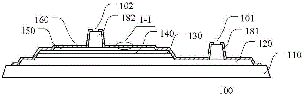
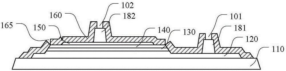
[0060] The passivation protection structure provided by the prior art and the present invention and its manufacturing method will be described in detail below with reference to the accompanying drawings and specific implementation examples. For the convenience of description and understanding, a relatively simple LED device with a front-mounted planar structure after the metal electrodes are fabricated is selected as the object that needs to be fabricated with a passivation protection structure.

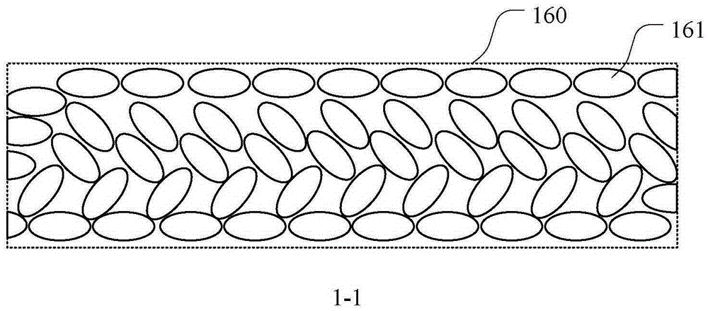
[0061] figure 1 and 2 A schematic cross-sectional view and a partially enlarged view of an LED device according to the prior art are respectively shown, wherein, figure 2...


PUM


Abstract

The invention discloses a passivation protecting structure, a light emitting diode and manufacturing methods thereof. The passivation protecting structure comprises a first passivation film, wherein the first passivation film is a single layer or laminated layers on at least a part of the surface of a semiconductor structure, and the single layer or each layer of the laminated layers of the first passivation film comprises at least one of a polymer layer with an insulation characteristic, an organic complex layer or a composite layer formed by the polymer layer and the organic complex layer. The passivation protecting structure adopts an organic passivation film for improving density, step coverage degree and adhesivity of the passivation film.

Description

technical field [0001] The present invention relates to a semiconductor device and a manufacturing method thereof, more specifically, to a passivation protection structure, a light emitting diode and a manufacturing method thereof. Background technique [0002] With the use of patterned substrates and the advancement of epitaxial technology, the crystal quality of the epitaxial layer in light-emitting diodes (LEDs) has been significantly improved. Correspondingly, the luminous efficiency of LED has been greatly improved, and has the advantages of health, energy saving and environmental protection in lighting applications. LED has been widely used in display screens, LCD backlights, traffic lights, outdoor lighting and other fields, and has begun to penetrate into indoor lighting, automotive lights, stage lights, special lighting and other fields. It is believed that in the near future, LEDs will fully replace traditional light sources. [0003] In the process of LED replac...

Claims


Application Information

Patent Timeline
Patent Type & Authority Applications(China)
IPC IPC(8): H01L33/56
CPCH01L33/56H01L2933/005
Inventor 江忠永马新刚李东昇丁海生
Owner HANGZHOU SILAN AZURE
Why Eureka
Try Eureka