Three-dimensional metallic grating making method

A fabrication method and metal grating technology, applied in directions such as diffraction gratings, can solve the problems of low light absorption efficiency of two-dimensional gratings, low electron transition and transport probability, sacrificing quantum wells, etc., so as to improve detection sensitivity and promote miniaturization. , the effect of improving the coupling efficiency

Active Publication Date: 2016-03-02
SUZHOU INST OF NANO TECH & NANO BIONICS CHINESE ACEDEMY OF SCI
View PDF3 Cites 3 Cited by
  • Summary
  • Abstract
  • Description
  • Claims
  • Application Information

AI Technical Summary

Problems solved by technology

Compared with the direct incidence method, the coupling efficiency is improved a lot, but this method will sacrifice part of the quantum well
[0004] In addition, the traditional surface periodic structure uses a two-dimensional structured grating. The incident light is reflected and diffracted to achieve light absorption. The light only passes through the absorption path twice in the quantum well layer, so the light absorption efficiency of the two-dimensional

Method used


Image

  • Three-dimensional metallic grating making method
  • Three-dimensional metallic grating making method

Examples


Embodiment Construction

[0018] Hereinafter, embodiments of the present invention will be described in detail with reference to the accompanying drawings. This invention may, however, be embodied in many different forms and should not be construed as limited to the specific embodiments set forth herein. Rather, the embodiments are provided to explain the principles of the invention and its practical application, thereby enabling others skilled in the art to understand the invention for various embodiments and with various modifications as are suited to particular intended uses.

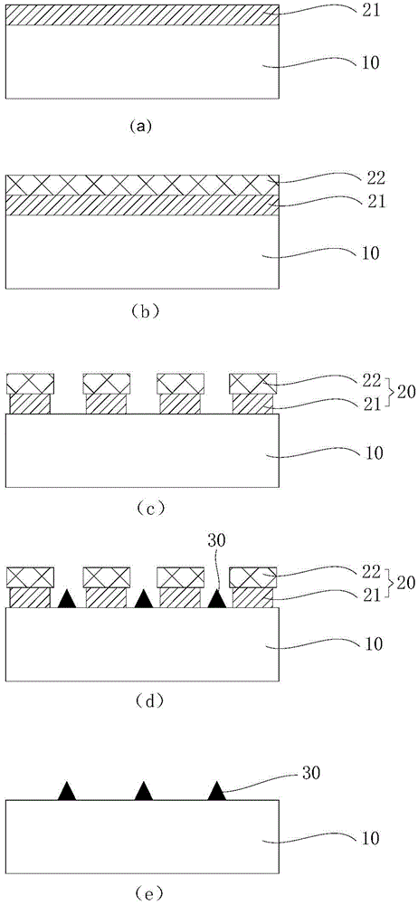
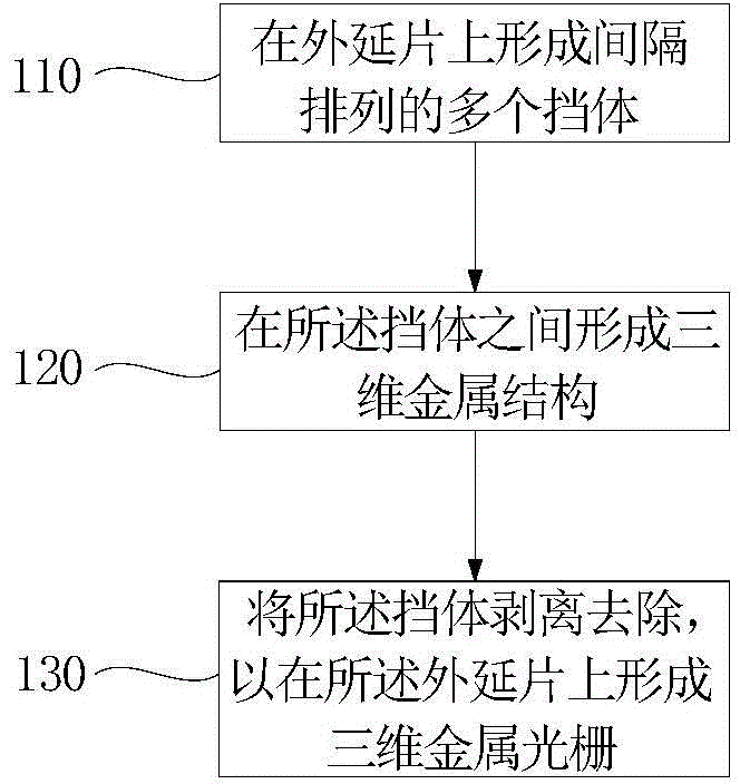
[0019] figure 1 is a flow chart of a method for manufacturing a three-dimensional metal grating according to an embodiment of the present invention. figure 2 is a structural schematic diagram of fabricating a three-dimensional metal grating according to an embodiment of the present invention.

[0020] refer to figure 1 , in step 110 , a plurality of barriers 20 arranged at intervals are formed on the epitaxial wafer 10 . ...


PUM


Abstract

The invention discloses a three-dimensional metallic grating making method. The method comprises steps: multiple blocking bodies arranged at intervals are formed on an epitaxial wafer; three-dimensional metallic structures are formed between the blocking bodies; the blocking bodies are stripped and removed to enable a three-dimensional metallic grating to be formed on the epitaxial wafer. Surface plasmon polaritons are used for restraining energy on the metallic surface, the electric field strength parallel to a quantum well material growth direction can be enhanced in a near field range, a thermal evaporation principle is adopted to prepare the three-dimensional metallic grating, and thus the coupling efficiency of multiple quantum wells on light is improved, the detection sensitivity of an infrared detector is improved, and the infrared detector system is promoted to be developed to the targets of miniature, portability and high sensitivity.

Description

technical field [0001] The invention belongs to the field of micro-nano processing and photoelectric sensors, and in particular relates to a method for manufacturing a three-dimensional metal grating. Background technique [0002] Quantum Well Infrared Photodetector (Quantum Well Infrared Photodetector, referred to as QWIP) can artificially cut the bandgap width by changing the potential well width and barrier height, so as to realize the controllable response wavelength. It has broad application prospects in medical and health fields, and has become a research hotspot in the field of infrared detectors in recent years. [0003] However, according to the limitation of quantum well subband transition selection rules, the incident photons perpendicular to the quantum well material cannot excite the ground state electronic transition in the QWIP quantum well, and the infrared radiation in the response band can only be absorbed through a certain angle of incidence or coupling. ...

Claims


Application Information

Patent Timeline
IPC IPC(8): G02B5/18
Inventor 曾春红付凯李晓伟林文魁陆增天张宝顺
Owner SUZHOU INST OF NANO TECH & NANO BIONICS CHINESE ACEDEMY OF SCI
Why Eureka
Try Eureka