A method for integrating vertical nanowire transistors
An integration method and nanowire technology, applied in nanotechnology, nanotechnology, nanotechnology for information processing, etc., can solve problems such as difficulty in using the gate-last process, limit the improvement of device performance, etc., to avoid etching damage, The effect of improving consistency and improving performance
- Summary
- Abstract
- Description
- Claims
- Application Information
AI Technical Summary
Problems solved by technology
Method used
Image

Examples
Embodiment 1
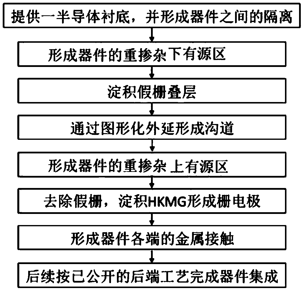
[0094] The CMOS integration of bulk silicon vertical nanowire devices with a diameter of 6nm can be realized according to the following steps (the structural parameters are set according to the High-Performance devices of the "11 / 10nm" technology generation in ITRS-2013):
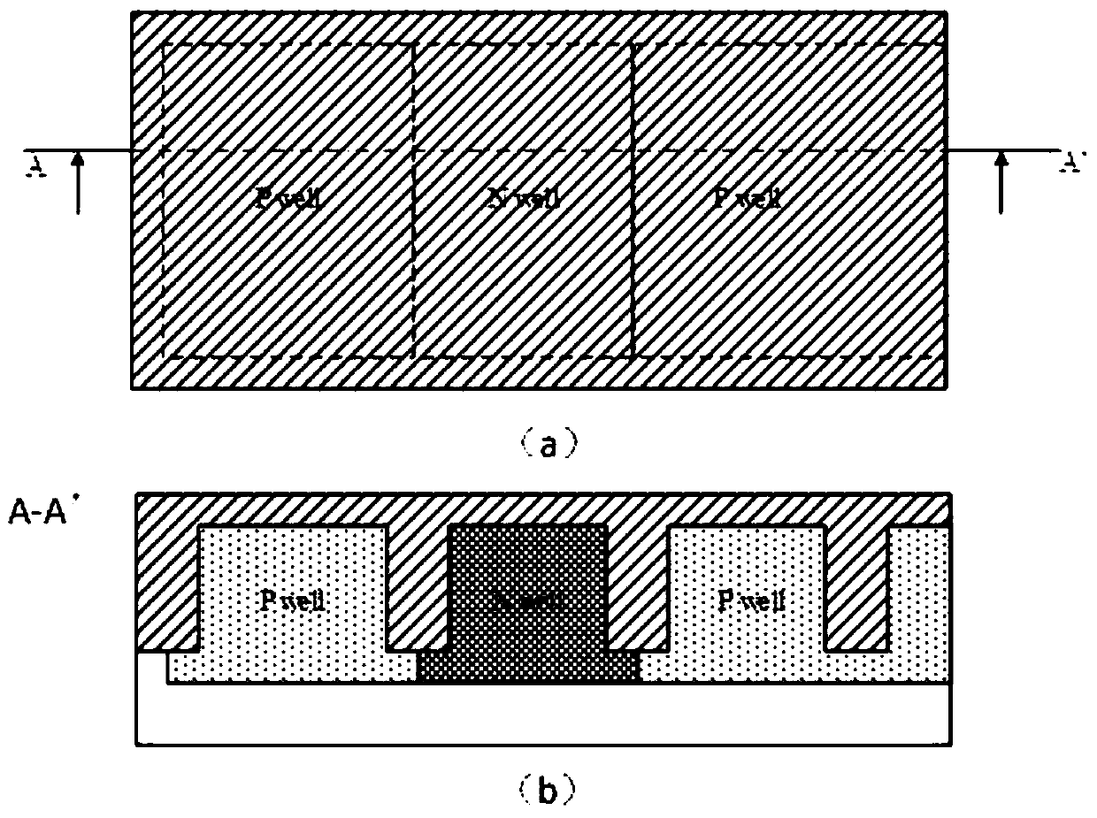
[0095] 1) On a (100) bulk silicon substrate, a double well (N well / P well), SiO 2 The shallow trench isolation (Shallow Trench Isolation, STI), the surface is planarized by chemical mechanical polishing (Chemical-MechanicalPolishing, CMP), and the substrate surface retains 50nm SiO 2 ,Such as figure 2 shown;
[0096] 2) Form the epitaxial window of the active region under the device by photolithography and anisotropic etching;
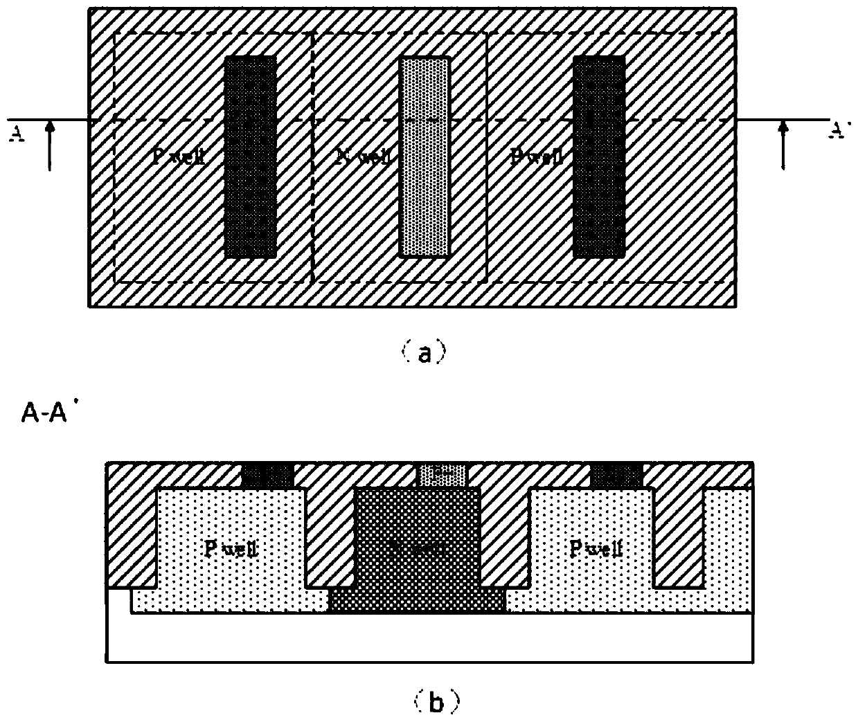
[0097] 3) The P+ heavily doped lower active region (as the source / drain terminal of PMOS) is formed on the N well by the epitaxial process of in-situ doping, and the N+ heavily doped lower active region is formed on the P well (as the NMOS source / drain), such as image 3 shown;...
Embodiment 2
[0121]According to the following steps, the hybrid integration of vertical nanowire devices (such as Si-NMOS and Ge-PMOS) with a diameter of 4.5nm of two kinds of material channels on the SOI substrate can be realized (the structural parameters are according to "8 / 7nm" in ITRS-2013 Technology generation High-Performance devices for setting):
[0122] 1) GeSi epitaxy 20nm on the (100) SOI substrate, respectively carry out N+ and P+ doping to form the lower active region of the device (as the source / drain terminal of the device);
[0123] 2) Realize the isolation of the active region under the N / P device by photolithography and etching, such as Figure 19 shown;
[0124] 3) SiO by LPCVD 2 STI is formed, and the surface is planarized by CMP to expose the upper surface of the heavily doped active region;
[0125] 4) Deposit 3nm SiO sequentially by ALD 2 (as SDE mask layer 1, its thickness defines the length of the source-drain extension region SDE of the device is 3nm), 14nm S...
PUM
 Abstract
Description
Claims
Application Information
 - R&D
- Intellectual Property
- Life Sciences
- Materials
- Tech Scout
- Unparalleled Data Quality
- Higher Quality Content
- 60% Fewer Hallucinations
Browse by: Latest US Patents, China's latest patents, Technical Efficacy Thesaurus, Application Domain, Technology Topic, Popular Technical Reports.
© 2025 PatSnap. All rights reserved.Legal|Privacy policy|Modern Slavery Act Transparency Statement|Sitemap|About US| Contact US: help@patsnap.com