Process for producing semiconductor devices, and semiconductor device

A manufacturing method and semiconductor technology, which are applied to the manufacture of semiconductor devices and the field of semiconductor devices, can solve problems such as poor moldability and poor flame retardancy of cured products, and achieve the effects of excellent moisture resistance reliability, improved production efficiency, and excellent balance.

Inactive Publication Date: 2016-03-02
SUMITOMO BAKELITE CO LTD
View PDF10 Cites 10 Cited by
  • Summary
  • Abstract
  • Description
  • Claims
  • Application Information

AI Technical Summary

Problems solved by technology

[0009] Patent Document 6 describes a sealant obtained by combining a silicone resin containing a phenyl group and a hydroxyl group or a phenyl group and a propyl group with a phenylaralkyl type, a biphenyl type, or a biphenylaralkyl type epoxy resin. An example of an epoxy resin composition is used, but if the silicone resin contains a large amount of hydroxyl groups, the molecular weight of the silicone resin will increase during molding and the viscosity will increase, resulting in poor moldability
In addition, since the silicone resin contains a long-chain alkyl group such as a propyl group, the flame retardancy of the cured product is significantly poor.

Method used


Image

  • Process for producing semiconductor devices, and semiconductor device
  • Process for producing semiconductor devices, and semiconductor device
  • Process for producing semiconductor devices, and semiconductor device

Examples


no. 1 approach >

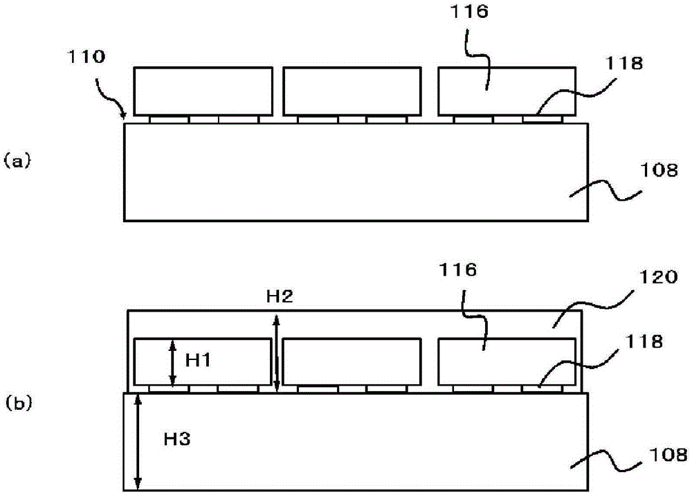
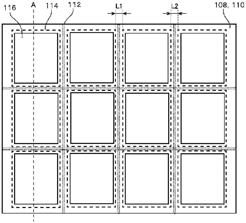
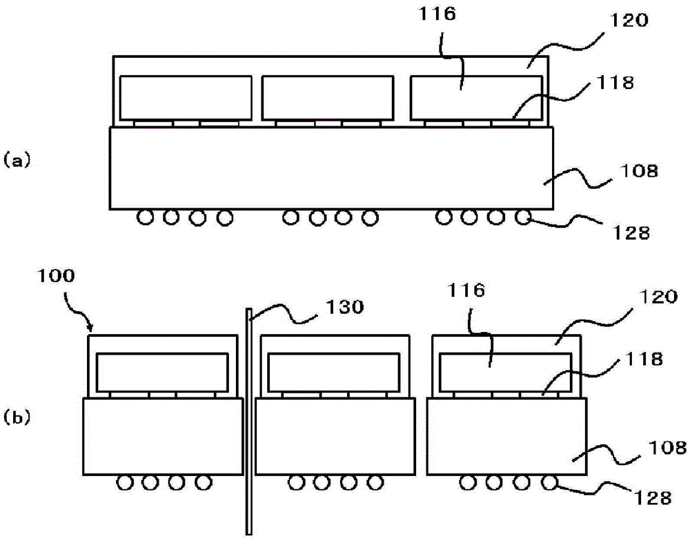
[0067] The manufacturing method of the semiconductor device 100 of this embodiment is called a so-called "MAP method" and includes the following steps. First, an element mounting substrate 108 including a plurality of packaging regions 114 partitioned by dicing regions 112 is prepared (hereinafter referred to as a preparation step). Then, the semiconductor chip 116 is mounted on each package area 114 of the element mounting substrate 108 (hereinafter referred to as a mounting step). Then, the semiconductor chip 116 is simultaneously molded with the epoxy resin composition for sealing (hereinafter, referred to as a molding process). Dicing is performed along the dicing region 112 to separate the individual molded semiconductor chips 116 (hereinafter referred to as a singulation process).

[0068] The epoxy resin composition for sealing of this embodiment contains (A) epoxy resin, (B) curing agent, (C) silicone resin, (D) inorganic filler, (E) curing accelerator, (C) organic T...

no. 2 approach >

[0239] Although the method of manufacturing a semiconductor device called the so-called "MAP method" in the first embodiment is shown, the above-mentioned epoxy resin composition for sealing can also be applied to electronic component assemblies (sometimes referred to as packaging or PKG) as exemplified below. ).

[0240] That is, Patent Document 7 shows an example of a single-sided sealed electronic component assembly for vehicle use, in which electronic components are mounted on one side of a circuit board and electrically connected to terminals of a lead frame with electric wires. The other side of the circuit board is bonded to the heat sink via the adhesive layer. A mold package in which terminals of these circuit boards, electronic components, heat sinks, and lead frames are sealed with a mold resin has been disclosed, and attempts have been made to prevent peeling by designing the package structure.

[0241] However, in the above-mentioned electronic components, if the...

Embodiment 1

[0342] Weigh epoxy resin 1 (8.00 parts by mass), phenolic curing agent 1 (5.00 parts by mass), inorganic filler 1 (75.00 parts by mass), inorganic filler 2 (10.00 parts by mass), hardening accelerator 4 (0.20 parts by mass), silane coupling agent 1 (0.20 parts by mass), release agent 1 (0.20 parts by mass), silicone resin 1 (1.00 parts by mass), colorant 1 (0.40 parts by mass), and mix them with a mixer Then, kneading was performed using two rolls whose surface temperatures were 95° C. and 25° C., thereby obtaining a kneaded product. Then, the epoxy resin composition for sealing of Example 1 was obtained by pulverizing this kneaded material after cooling.


PUM

PropertyMeasurementUnit
softening pointaaaaaaaaaa
particle sizeaaaaaaaaaa

Abstract

A process for semiconductor device production which comprises: a preparation step in which a substrate for element mounting (108) equipped with a plurality of package areas (114) separated by dicing regions (112) is prepared; a mounting step in which semiconductor chips (116) are mounted respectively on the package areas (114) of the substrate for element mounting (108); a molding step in which the semiconductor chips (116) are simultaneously encapsulated by molding with an encapsulating epoxy resin composition; and a chip formation step in which the resultant structure is diced along the dicing regions (112) to separate the individual encapsulated semiconductor chips (116). The encapsulating epoxy resin composition comprises (A) an epoxy resin, (B) a hardener, (C) a silicone resin, (D) an inorganic filler, and (E) a hardening accelerator, wherein the silicone resin (C) is a branched silicone resin that is a methylphenyl-type thermoplastic silicone resin and has repeating structural units represented by general formulae (a), (b), (c), and (d). (In the formulae, symbol * indicates a bond with the Si atom contained in a repeating structural unit of another or the same kind; and R1a, R1b, R1c, and R1d are each a methyl or phenyl group and may be the same as or different from one another. The content of Si-bonded phenyl groups is 50 mass% or higher of the molecule, and the content of Si-bonded OH groups is less than 0.5 mass% of the molecule.) The formulae is shown in the specification.

Description

technical field [0001] The present invention relates to a method of manufacturing a semiconductor device and a semiconductor device. Background technique [0002] In recent years, in the technical field of semiconductor packaging, small packages such as CSP (Chip Size Package) and BGA have been used in order to meet demands such as miniaturization and multi-pin increase. [0003] As for their packaging method, the MAP (Mold Array Package) method that can greatly reduce the mounting area and manufacturing cost by grouping semiconductor chips into modules by a batch molding method is adopted. The MAP method refers to a production method in which dozens of chips are arranged in a matrix on a large substrate, sealed in batches on one side, and then diced into individual packages (for example, refer to Patent Document 1 and Patent Document 2). [0004] In addition, in recent years, the high integration, high-density mounting, and high-power of electronic components have been dev...

Claims


Application Information

Patent Timeline
Patent Type & Authority Applications(China)
IPC IPC(8): C08L63/00C08G59/62C08L83/05C08L83/06
CPCC08L63/00C08G59/621C08G77/80C08L83/04
Inventor 田部井纯一
Owner SUMITOMO BAKELITE CO LTD
Why Eureka
Try Eureka