A detector based on semiconductor laser and its parameter adjustment method
A parameter adjustment and laser technology, applied in the field of spectral detection, can solve the problems of affecting the analysis results, reducing sensitivity, and high price, and achieve the effect of improving speed and efficiency, reducing dependence, and low price
- Summary
- Abstract
- Description
- Claims
- Application Information
AI Technical Summary
Problems solved by technology
Method used
Image
Examples
no. 1 example
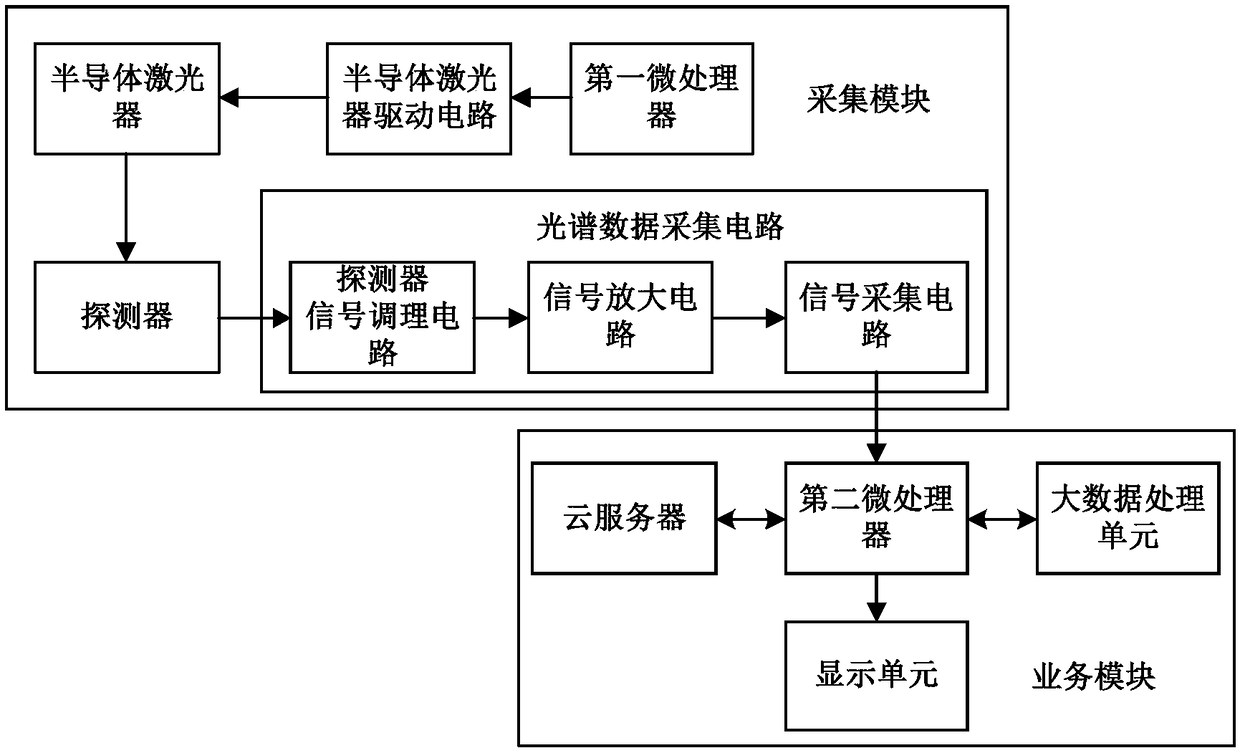
[0094] The intelligent cloud detector of the present invention adopts a modular design and can be divided into three modules, namely, a business module, a collection module and a sample module. Both the business module and the acquisition module have a unique dedicated microprocessor for data processing. The three modules are introduced one by one below.
[0095] (1) Sample module
[0096] The sample module is mainly used to load samples, and its structure is as follows Figure 4 Shown, includes sample cup, cup holder, and turret.
[0097] Among them, the sample cup is used for loading samples.
[0098] The cup holder is arranged on the left side of the sample cup and is used to support the sample cup.
[0099] The turntable is arranged under the sample cup, and is used to evenly distribute the sample by rotating (the sample may be powdery and may be unevenly distributed), so that the collected data is more accurate.
[0100] (2) Acquisition module
[0101] The collectio...
no. 2 example
[0121] The parameter adjustment method of the intelligent cloud detector of the present invention mainly includes the following two parts: (1) adjusting the parameters of the optical path of the semiconductor laser of the acquisition module; (2) optimizing the whole system of the intelligent cloud detector. The two parts are described one by one below.
[0122] (1) Adjust the parameters of the optical path of the semiconductor laser of the acquisition module
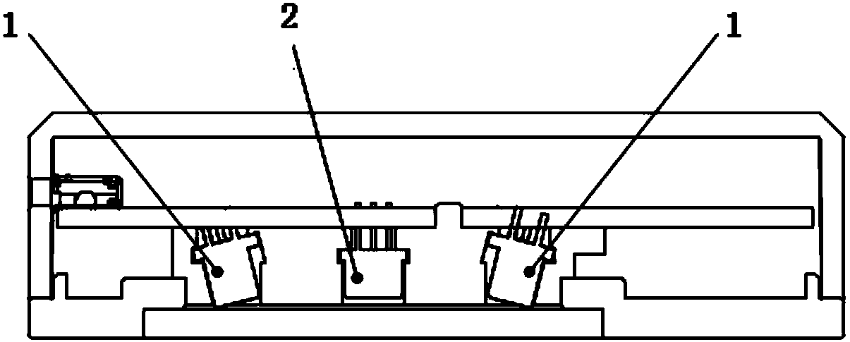
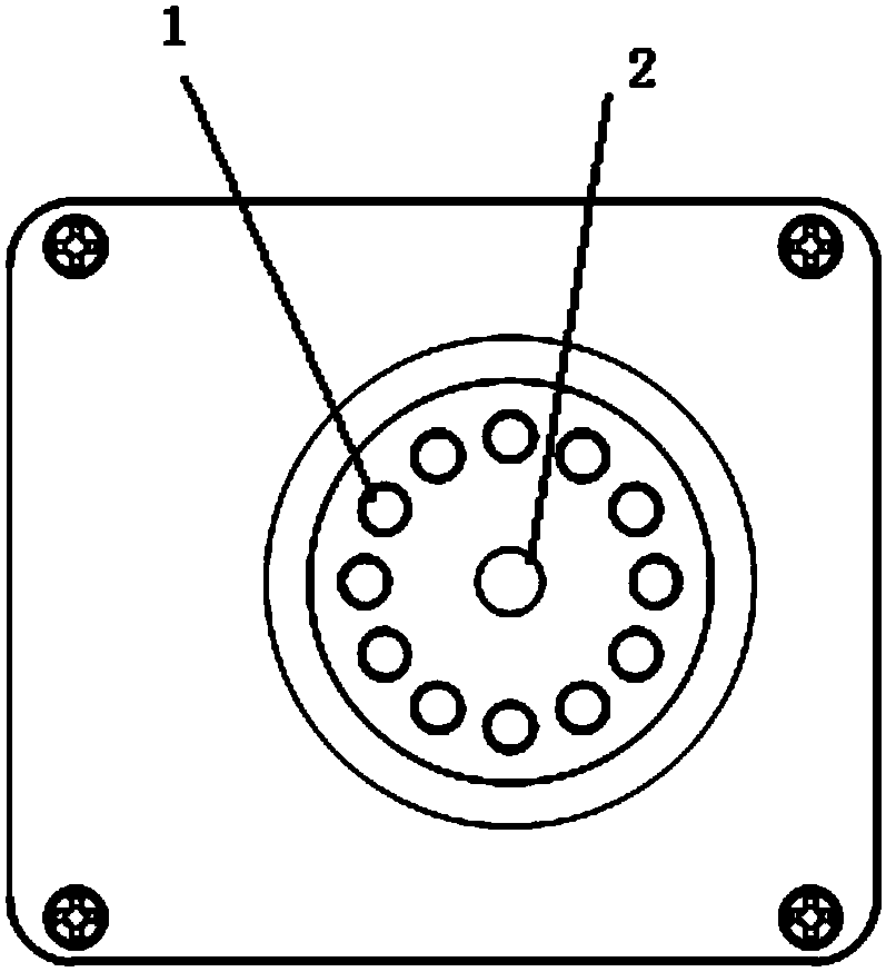
[0123] The optical path design of the acquisition module is centered on the detector, and the semiconductor laser is distributed on a circle. There is a certain horizontal distance D between the semiconductor laser and the detector, and there is a certain vertical distance K between the detector and the sample in the sample module. The semiconductor laser and the horizontal plane There must be a certain angle α, so that the light spots emitted by each laser can coincide with the sample, such as Figure 4 shown.
[0124...
PUM
 Abstract
Description
Claims
Application Information
 - R&D
- Intellectual Property
- Life Sciences
- Materials
- Tech Scout
- Unparalleled Data Quality
- Higher Quality Content
- 60% Fewer Hallucinations
Browse by: Latest US Patents, China's latest patents, Technical Efficacy Thesaurus, Application Domain, Technology Topic, Popular Technical Reports.
© 2025 PatSnap. All rights reserved.Legal|Privacy policy|Modern Slavery Act Transparency Statement|Sitemap|About US| Contact US: help@patsnap.com


