

Semiconductor structure and method of forming same, method of processing semiconductor structure
A processing method and semiconductor technology, applied in semiconductor devices, semiconductor/solid-state device manufacturing, microstructure technology, etc., can solve problems such as easy formation of fragments, cost loss, scrapping of MEMS devices, etc.
- Summary
- Abstract
- Description
- Claims
- Application Information
AI Technical Summary
Problems solved by technology
Method used
Image

Examples
Embodiment Construction
[0038] As mentioned in the background art, thin wafers formed with MEMS thin films are prone to breakage during wet processing.
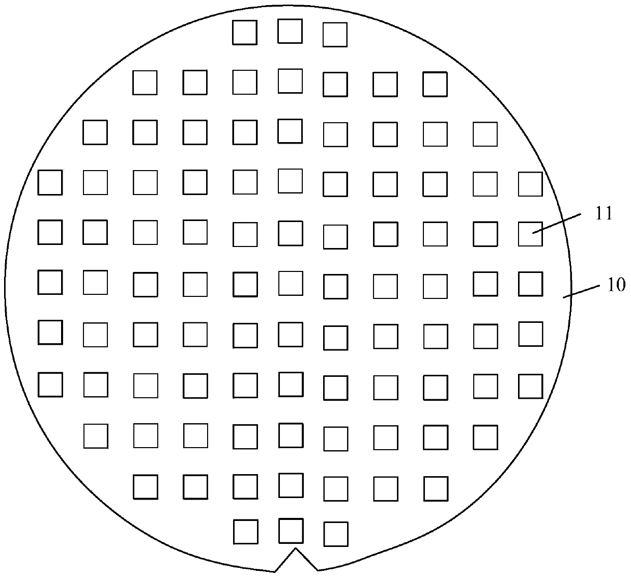
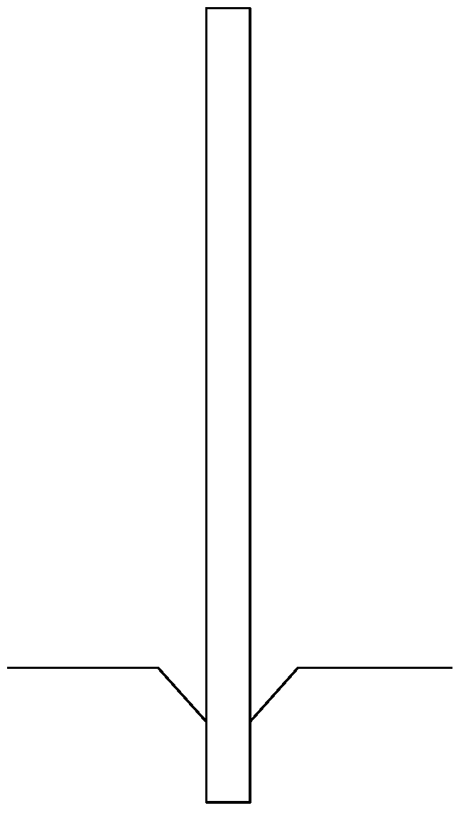
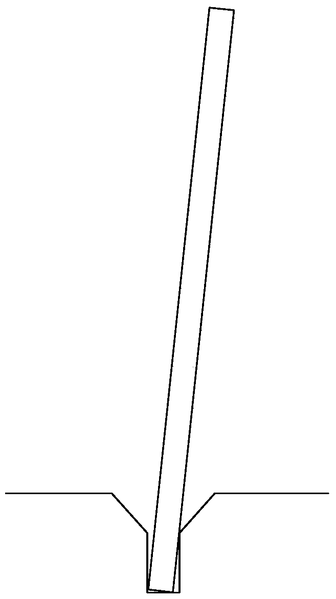
[0039] It was found that during wet processing, wafers are usually placed vertically on a wafer holder to facilitate simultaneous processing of multiple wafers. There are a plurality of guide grooves on the wafer guide frame, the thickness of the grooves is usually closer to the thickness of the wafer, and the wafer is vertically placed in the guide grooves, and the position is fixed (please refer to figure 2 ), able to maintain a vertical state. However, after thinning the wafer with the MEMS thin film, the thickness of the wafer drops a lot. When the subsequent wet process is performed, the thickness of the thinned wafer is quite different from the size of the groove, so that the wafer is in the wafer. The position on the round guide frame cannot be fixed, and it is easy to tilt (please refer to image 3 ), and when a wafer is tilted, it is eas...
PUM
| Property | Measurement | Unit |
|---|---|---|
| width | aaaaa | aaaaa |
| thickness | aaaaa | aaaaa |
Abstract
Description
Claims
Application Information