Acid-washing process for diode chip

A diode and secondary pickling technology, applied in the field of diodes, can solve the problems of secondary pollution, dissolution, and affecting product quality, and achieve the effect of reducing metal ions, improving electrical properties and high-temperature electrical properties

Inactive Publication Date: 2016-03-23
RUGAO DACHANG ELECTRONICS
View PDF6 Cites 6 Cited by
  • Summary
  • Abstract
  • Description
  • Claims
  • Application Information

AI Technical Summary

Problems solved by technology

[0003] At present, the cleaning solution in the primary pickling is a mixture of nitric acid, sulfuric acid, hydrofluoric acid and glacial acetic acid; there are two types of cleaning solutions in the secondary pickling: 1. A mixture of phosphoric acid, hydrogen peroxide and water. Disadvantages: there is Pb in the solder, During a pickling, it will react with sulfuric acid in the cleaning solution to form PbSO 4 , lead sulfate is an insoluble substance, it will be adsorbed on the surface of the chip, and the pickling solution cannot remove the PbSO adsorbed on the surface of the chip 4 2. The mixture of phosphoric acid, hydrogen peroxide, water and glacial acetic acid, with a volume ratio of 1:0.8:3:0.2, can dissolve PbSO on the surface of the chip 4 , reduce the free metal ions on the surface of the chip, improve its electrical performance at room temperature and high temperature electrical performance, disadvantages: the residual glacial acetic acid contains high metal content, which will cause secondary pollution, thereby reducing electrical performance

Method used


Image

  • Acid-washing process for diode chip

Examples


Embodiment 1

[0012] The pickling process of the diode chip in this embodiment, the specific steps of the pickling process are as follows:

[0013] (1) Pickling once: place the diode chip in HNO with a volume ratio of 9:9:12:4 3 , HF, CH 3 COOH and H 2 SO 4 Pickling in the mixed solution for 115s;

[0014] (2) Second pickling: The diode chip after the first pickling is re-used with H with a volume ratio of 1:0.4:3:0.4 3 PO 4 、H 2 o 2 、H 2 O and CH 3 Pickling with COOH mixed solution for 75s;

[0015] (3) Cleaning with hydrogen peroxide and ammonia water: use NH with a volume ratio of 2:1:5 for the diode chip after the second pickling 3 . h 2 O, H 2 O and H 2 o 2 Wash for 3 minutes;

[0016] (4) Ultrasonic cleaning with water: finally, ultrasonically clean the above-mentioned diode chip with water for 8 minutes.

Embodiment 2

[0018] The pickling process of the diode chip in this embodiment, the specific steps of the pickling process are as follows:

[0019] (1) Pickling once: place the diode chip in HNO with a volume ratio of 9:9:12:4 3 , HF, CH 3 COOH and H 2 SO 4 Pickling in the mixed solution for 125s;

[0020] (2) Second pickling: The diode chip after the first pickling is re-used with H with a volume ratio of 1:0.4:3:0.4 3 PO 4 、H 2 o 2 、H 2 O and CH 3 Pickling with COOH mixed solution for 73s;

[0021] (3) Cleaning with hydrogen peroxide and ammonia water: use NH with a volume ratio of 2:1:5 for the diode chip after the second pickling 3 . h 2 O, H 2 O and H 2 o 2 Wash for 2 minutes;

[0022] (4) Ultrasonic cleaning with water: Finally, ultrasonically clean the diode chip with water for 5 minutes.

Embodiment 3

[0024] The pickling process of the diode chip in this embodiment, the specific steps of the pickling process are as follows:

[0025] (1) Pickling once: place the diode chip in HNO with a volume ratio of 9:9:12:4 3 , HF, CH 3 COOH and H 2 SO 4 Pickling in the mixed solution for 120s;

[0026] (2) Second pickling: The diode chip after the first pickling is re-used with H with a volume ratio of 1:0.4:3:0.4 3 PO 4 、H 2 o 2 、H 2 O and CH 3 Pickling with COOH mixed solution for 74s;

[0027] (3) Cleaning with hydrogen peroxide and ammonia water: use NH with a volume ratio of 2:1:5 for the diode chip after the second pickling 3 . h 2 O, H 2 O and H 2 o 2 Wash for 2.5 minutes;

[0028] (4) Ultrasonic cleaning with water: finally, ultrasonically clean the above-mentioned diode chip with water for 6 minutes.

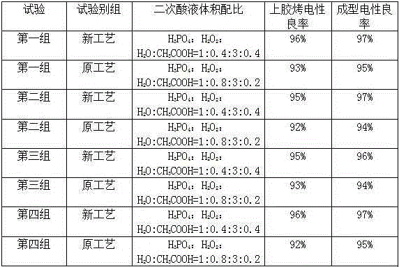
[0029] Secondary pickling solution H in embodiments 1 to 3 3 PO 4 、H 2 o 2 、H 2 O and CH 3 The configuration of the COOH mixture is: add water first, then ...


PUM


Abstract

The invention relates to a production process for diodes. The production process comprises five steps of acid washing, electroplating, welding, insulation protection and post-treatment. The production process for the diodes has the advantages that the steps of acid washing, welding and welding are performed in sequence; a chip is subjected to acid corrosion before welding, so that solders and metal impurities in lead wires are prevented from reacting with an acid liquid to influence a corrosive rate of the chip in the acid washing process; metal ions generated by reaction of metal and acid are prevented from being adhered to the surface of the chip, so that large amounts of washing processes are removed and resources are saved; the faults such as electric degradation and high-temperature thermal breakdown of a product are avoided, so that the electric yield of the product is increased; and meanwhile, the metal content of a discharged washing liquid is reduced and the soil pollution is alleviated, so that the environmental protection is facilitated.

Description

technical field [0001] The invention relates to the field of diodes, in particular to a pickling process for diode chips. Background technique [0002] According to the principle of diode semiconductor production, when the chip is to function, it must undergo acid corrosion and acid passivation. The pickling process of the diode chip includes one pickling, two pickling, mixed cleaning with ammonia water and hydrogen peroxide, and finally ultrasonic cleaning with water. [0003] At present, the cleaning solution in the primary pickling is a mixture of nitric acid, sulfuric acid, hydrofluoric acid and glacial acetic acid; there are two types of cleaning solutions in the secondary pickling: 1. A mixture of phosphoric acid, hydrogen peroxide and water. Disadvantages: there is Pb in the solder, During a pickling, it will react with sulfuric acid in the cleaning solution to form PbSO 4 , lead sulfate is an insoluble substance, it will be adsorbed on the surface of the chip, and t...

Claims


Application Information

Patent Timeline
Patent Type & Authority Applications(China)
IPC IPC(8): H01L21/02B08B3/08
CPCB08B3/08H01L21/02057H01L21/02082
Inventor 黄丽凤
Owner RUGAO DACHANG ELECTRONICS
Why Eureka
Try Eureka