Semiconductor structure forming method

A semiconductor and conductive layer technology, which is applied in semiconductor/solid-state device manufacturing, electrical components, circuits, etc., can solve problems such as differences in electrical properties of conductive plugs, unstable electrical properties of conductive films, etc.

Active Publication Date: 2016-03-30
SEMICON MFG INT (SHANGHAI) CORP
View PDF5 Cites 0 Cited by
  • Summary
  • Abstract
  • Description
  • Claims
  • Application Information

AI Technical Summary

Problems solved by technology

[0008] However, since the electrical properties of the formed conductive film are unstable, there are differences in the electrical properties of the conductive plugs formed from the conductive film.

Method used


Image

  • Semiconductor structure forming method
  • Semiconductor structure forming method
  • Semiconductor structure forming method

Examples


Embodiment Construction

[0037] As described in the prior art, due to the unstable electrical properties of the formed conductive film, the electrical properties of the conductive plugs formed by the conductive film are different.

[0038] After research, it is found that due to the limitation of the physical vapor deposition process, the electrical thickness of the conductive film formed on the surface of different substrates is different, resulting in differences in the electrical properties of the conductive plug formed by the conductive film, resulting in differences between the substrates. The electrical connection performance is not stable.

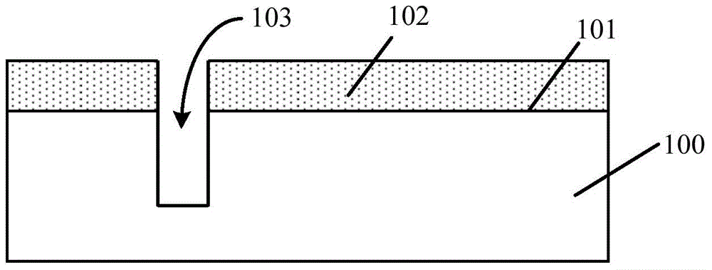
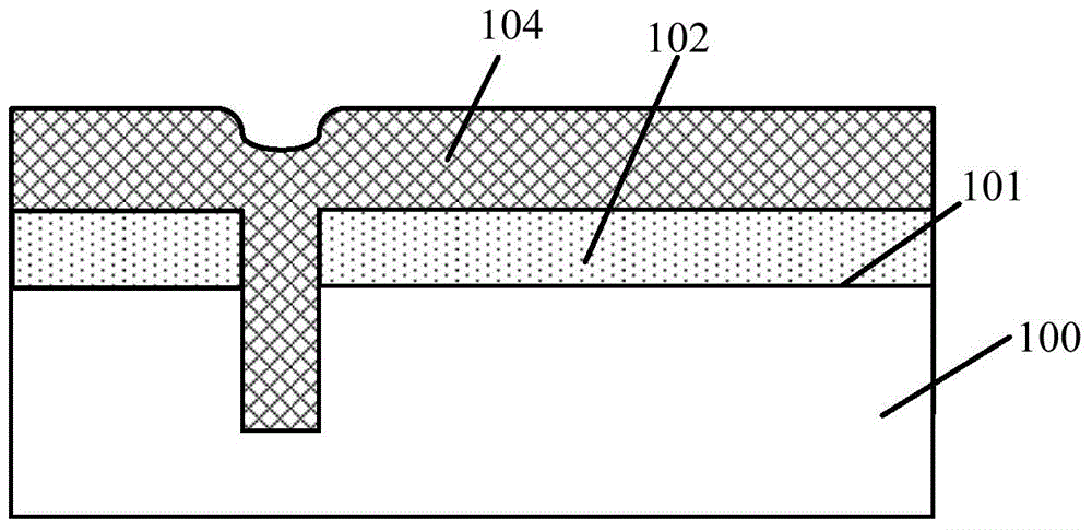
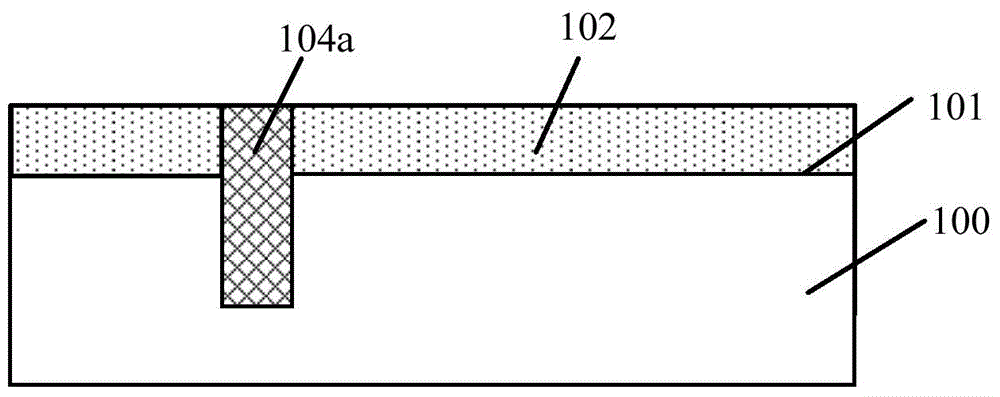
[0039] Please continue to refer Figure 1 to Figure 3 , since the device layer 102 is formed on the surface of the substrate 100 before the conductive film 104 is formed, in order to avoid damage to the device layer 102 caused by the process of forming the conductive film 104, the temperature of the physical vapor deposition process needs to be The temperat...


PUM

PropertyMeasurementUnit
Thicknessaaaaaaaaaa

Abstract

The invention discloses a semiconductor structure forming method, and the method comprises the steps: providing a plurality of substrates, wherein each substrate is provided with a first surface and a second surface opposite to the first surface, and the first surface of each substrate is provided with a device layer; providing physical vapor deposition equipment which comprises a pre-treatment cavity and a technological cavity, wherein the pre-treatment cavity and the technological cavity are connected with each other; placing the plurality of substrates into the technological cavity, and forming a conductive layer on the second surface of each substrate or on the surface of each device layer through employing the technology of physical vapor deposition; enabling the plurality of substrates to be placed in the pre-treatment cavity after the conductive layer is formed, and carrying out the annealing of the conductive layer. The formed conductive layer is uniform in electric thickness, and is stable in electrical performance.

Description

technical field [0001] The invention relates to the technical field of semiconductor manufacturing, in particular to a method for forming a semiconductor structure. Background technique [0002] In the field of semiconductor manufacturing, in order to realize the electrical connection between semiconductor devices, various metal interconnection structures and formation processes have been developed. For example, the physical vapor deposition (Physical Vapor Deposition, PVD) Or aluminum-copper (AlCu) alloy as the material of the electrical interconnection structure. However, with the development of Ultra Large Scale Integration (ULSI), the process of forming metal interconnection structures is also challenged. [0003] Taking the existing Through Silicon Via (TSV for short) structure as an example, Figure 1 to Figure 3 It is a schematic cross-sectional structure diagram of the formation process of the TSV structure in the prior art. [0004] Please refer to figure 1 , pr...

Claims


Application Information

Patent Timeline
IPC IPC(8): H01L21/02
Inventor 陈怡骏冯健游宽结
Owner SEMICON MFG INT (SHANGHAI) CORP
Why Eureka
Try Eureka