

Graphene LED chip and preparation method thereof
An LED chip and graphene technology, applied in electrical components, circuits, semiconductor devices, etc., can solve the problems of poor light transmittance and conductivity, and the inability to make GaN electrodes, and achieves low absorption, thin overall thickness, and high emission. rate effect
- Summary
- Abstract
- Description
- Claims
- Application Information
AI Technical Summary
Problems solved by technology
Method used
Image

Examples
Embodiment 1
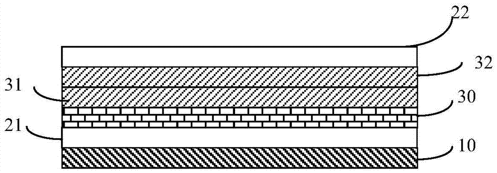
[0049] Such as figure 1 As shown, the present invention provides a graphene LED chip, comprising a substrate 10, a graphene transparent lower electrode 21, a graphene layer 30 with a superlattice structure, a P-type semiconductor layer 31, an N-type semiconductor layer 32, and graphene transparent The upper electrode 22.
[0050] The graphene layer 30 with a superlattice structure is disposed between the graphene transparent lower electrode 21 and the P-type semiconductor layer 31 . The N-type semiconductor layer 32 is disposed on the P-type semiconductor layer 31 . The graphene transparent upper electrode 22 is disposed above the N-type semiconductor layer 32 . That is, the N-type semiconductor layer 32 is disposed between the P-type semiconductor layer 31 and the graphene transparent upper electrode 22 .
[0051] The substrate 10 is a glass substrate, a quartz substrate, a silicon substrate, a plastic substrate, and a substrate composed of a combination of materials such ...
Embodiment 2
[0059] This embodiment provides a method for preparing a graphene LED chip.
[0060] Firstly, a graphene film is prepared. A high-purity graphite powder layer is coated on a quartz sheet, and the quartz sheet coated with the graphite powder layer is placed in a tubular boiler. The vacuum degree of the boiler is about 10 -5 Thor. The quartz sheet coated with the graphite powder layer is heat-treated at a temperature of 1200° C., so that the graphite powder layer forms a graphene layer. After the boiler is slowly cooled, the graphene layer coated on the quartz sheet can be torn off from the cooled quartz sheet to obtain a graphene layer containing stacked multilayer graphene films.
[0061] Then prepare the graphene LED chip. Such as Figure 7 Shown, the step of preparing graphene LED chip is:
[0062] S11: immersing the graphene layer containing the stacked multi-layer graphene film in an aqueous sulfuric acid solution to separate layers of the stacked graphene film to ob...
Embodiment 3
[0080] This embodiment is a further improvement on any of the foregoing embodiments, and only the improved part will be described.
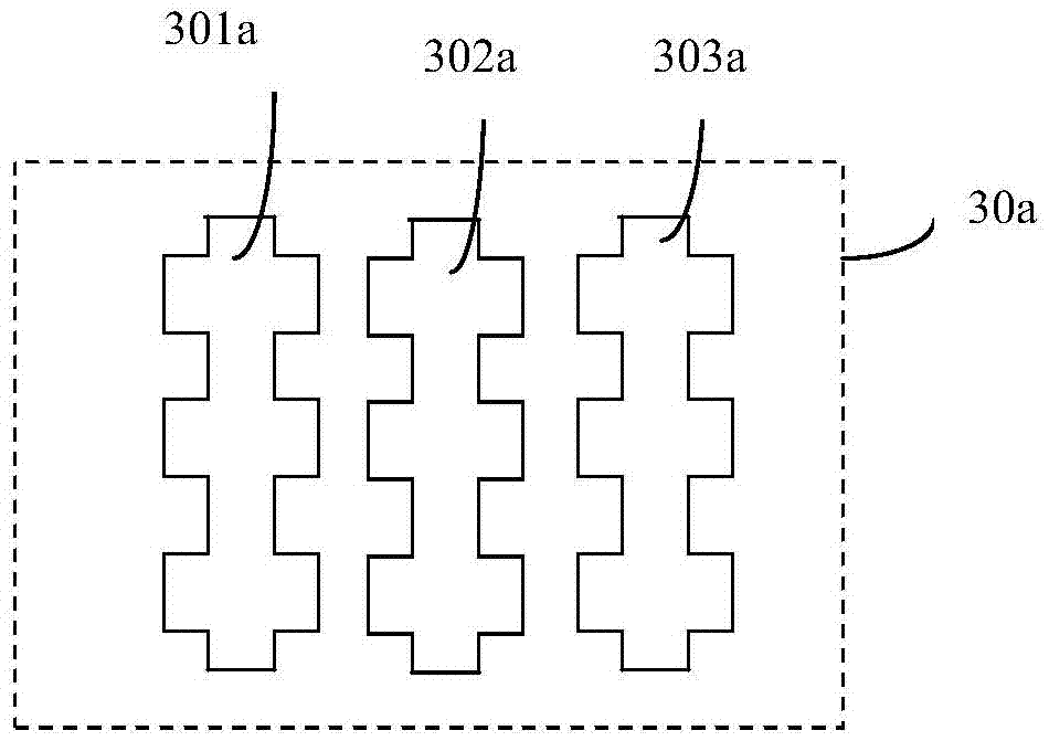
[0081] According to a preferred embodiment, the graphene layer with superlattice structure comprises at least one graphene nanoribbon. The graphene layer with the superlattice structure is connected with the graphene transparent upper electrode and the P-type semiconductor layer and has a band shape.
[0082] The graphene nanoribbon layer 30a has at least one graphene nanoribbon. Opposite edges of the graphene nanoribbons may have a zigzag shape. The graphene nanoribbons have periodically varying widths along the longitudinal direction. figure 2 Three nanoribbons 301a, 302a and 303a in graphene nanoribbon layer 30a are shown. Opposite edges of the graphene nanoribbon 301a each have a zigzag shape. The graphene nanoribbons 301a have periodically varying widths along the longitudinal direction.
[0083] The present invention is not limited th...
PUM
| Property | Measurement | Unit |
|---|---|---|
| Diameter | aaaaa | aaaaa |
| Thickness | aaaaa | aaaaa |
| Diameter | aaaaa | aaaaa |
Abstract
Description
Claims
Application Information