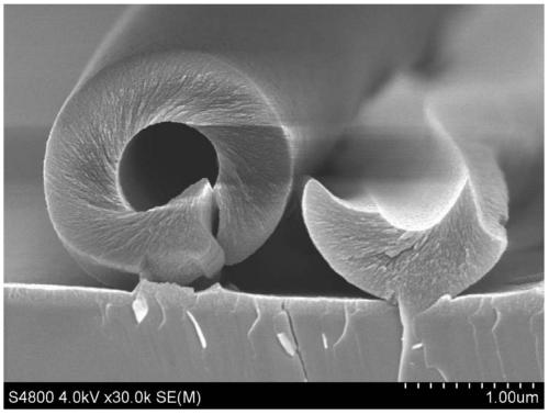
A kind of diamond-like microtube and its preparation method
A diamond and microtube technology, which is applied in metal material coating process, vacuum evaporation plating, coating and other directions, can solve the problem of difficulty in preparing microtube structures, and achieves a simple and easy preparation method, easy operation and good application prospect. Effect
- Summary
- Abstract
- Description
- Claims
- Application Information
AI Technical Summary
Problems solved by technology
Method used
Image
Examples
preparation example Construction
[0022] The invention provides a kind of preparation method of diamond-like micropipe, it comprises the following steps:
[0023] S1, providing a substrate, and performing surface etching treatment on the substrate;
[0024] S2, using magnetron sputtering and linear ion beam co-deposition to deposit a metal-doped diamond-like carbon film on the surface of the etched substrate; and
[0025] S3, soaking the substrate deposited with the metal-doped diamond-like carbon film in an acidic solution for a period of time, so that the metal in the metal-doped diamond-like carbon film is dissolved, and the diamond-like carbon film is formed under the action of compressive stress Crimping occurs, resulting in diamond-like microtubules with hollow structures.
[0026] In step S1, the surface of the substrate is cleaned by performing surface etching treatment on the substrate. The material of the substrate may be silicon, polyethylene terephthalate (abbreviated as PET), polypropylene (abbr...
Embodiment 1
[0041] Firstly, the surface etching treatment is carried out on the silicon substrate, specifically: put the silicon substrate into the chamber and start vacuuming, when the vacuum degree reaches 2.0×10 -5 When Pa, argon gas is introduced into the cavity, and the flow rate of argon gas is 35 sccm. At the same time, a pulsed negative bias voltage of 100V is applied to the silicon substrate, and the linear ion source is turned on. The operating current of the linear ion source is 0.2A. The surface of the substrate is etched for 10 minutes.
[0042] Then magnetron sputtering and linear ion beam co-deposition are used to deposit a copper-doped diamond-like carbon film on the surface of the etched substrate. Specifically: after the etching is completed, adjust the flow rate of argon gas to 65 sccm, and continue to feed Acetylene gas with a flow rate of 15 sccm, turn on the magnetron sputtering source and the linear ion beam source, wherein the operating current of the magnetron spu...
Embodiment 2
[0046] Firstly, the surface etching treatment is carried out on the silicon substrate, specifically: put the silicon substrate into the chamber and start vacuuming, when the vacuum degree reaches 2.0×10 -5 When Pa, argon gas is introduced into the cavity, and the flow rate of argon gas is 35 sccm. At the same time, a pulsed negative bias voltage of 100V is applied to the silicon substrate, and the linear ion source is turned on. The operating current of the linear ion source is 0.2A. The surface of the substrate is etched for 10 minutes.
[0047] Then magnetron sputtering and linear ion beam co-deposition are used to deposit an aluminum-doped diamond-like carbon film on the surface of the etched substrate. Specifically: after the etching is completed, the flow rate of argon gas is adjusted to 65 sccm, and the flow is continued. Acetylene gas with a flow rate of 15 sccm, turn on the magnetron sputtering source and the linear ion beam source, wherein the operating current of the...
PUM
| Property | Measurement | Unit |
|---|---|---|
| Diameter | aaaaa | aaaaa |
| Thickness | aaaaa | aaaaa |
| Diameter | aaaaa | aaaaa |
Abstract
Description
Claims
Application Information
 - R&D
- Intellectual Property
- Life Sciences
- Materials
- Tech Scout
- Unparalleled Data Quality
- Higher Quality Content
- 60% Fewer Hallucinations
Browse by: Latest US Patents, China's latest patents, Technical Efficacy Thesaurus, Application Domain, Technology Topic, Popular Technical Reports.
© 2025 PatSnap. All rights reserved.Legal|Privacy policy|Modern Slavery Act Transparency Statement|Sitemap|About US| Contact US: help@patsnap.com

