Polycrystal silicon preparation method

A polysilicon preparation and polysilicon technology, which is applied in semiconductor/solid-state device manufacturing, electrical components, circuits, etc., can solve the problems of abnormal etching of polysilicon graph lines, abnormal coating of photoresist at particle points, etc., to improve surface flatness, Effect of improving grain uniformity and reducing size

Inactive Publication Date: 2016-04-27
SHANGHAI HUALI MICROELECTRONICS CORP
View PDF6 Cites 8 Cited by
  • Summary
  • Abstract
  • Description
  • Claims
  • Application Information

AI Technical Summary

Problems solved by technology

Abnormal grain growth in photolithography will lead to abnormal photoresist coating at the particle point, which will lead to abnormal etching of polysilicon pattern lines during the etching process, resulting in linebroken (broken line)

Method used


Image

  • Polycrystal silicon preparation method
  • Polycrystal silicon preparation method

Examples


Embodiment Construction

[0030] The specific embodiment of the present invention will be further described in detail below in conjunction with the accompanying drawings.

[0031] It should be noted that, in the following specific embodiments, when describing the embodiments of the present invention in detail, in order to clearly show the structure of the present invention for the convenience of description, the structures in the drawings are not drawn according to the general scale, and are drawn Partial magnification, deformation and simplification are included, therefore, it should be avoided to be interpreted as a limitation of the present invention.

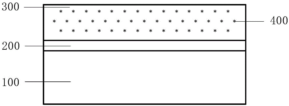
[0032] In the following specific embodiments of the present invention, please refer to figure 1 , figure 1 It is a schematic diagram of the polysilicon process structure formed according to a polysilicon preparation method of the present invention in a preferred embodiment of the present invention. Such as figure 1 Shown, a kind of polysilicon pre...


PUM


Abstract

The invention discloses a polycrystal silicon preparation method, which comprises the steps of: introducing a small amount of N2O into a reaction chamber body as a doping gas when carrying out a polycrystal silicon deposition process, so that the N2O reacts with SiH4 serving as a process gas to generate SiO2; and doping polycrystal silicon, wherein excessive part of the SiH4 continues to decompose to generate polycrystal silicon. The presence of the SiO2 inhibits abnormal grain growth in the polycrystal silicon deposition process, thus size of polycrystal silicon grains can be reduced, grain uniformity can be increased and surface evenness can be improved, thereby eliminating the problem of polycrystal silicon particle production.

Description

technical field [0001] The invention relates to the technical field of semiconductor integrated circuit manufacturing, and more particularly relates to a method for preparing polysilicon that can reduce the grain size. Background technique [0002] There are three types of silicon materials classified according to crystal orientation, namely: [0003] 1) Single crystal silicon (SinglecrystalSilicon): its crystal lattice is a regular and simple repeating form; [0004] 2) Polycrystalline Silicon (Polycrystalline Silicon): It is composed of different grains, and the lattice inside each grain is in a regular and simple repeating form; [0005] 3) Amorphous Silicon (AmorphousSilicon): Its lattice is in a freely distributed form. [0006] Among them, polysilicon material has been widely used in integrated circuits, and it can be used as transistor gate electrode (transistor gate electrode), circuit interconnection (interconnectionIncircuits), resistor (resistor) and so on. [...

Claims


Application Information

Patent Timeline
Patent Type & Authority Applications(China)
IPC IPC(8): H01L21/205H01L21/02
CPCH01L21/02532H01L21/0257H01L21/02595H01L21/0262
Inventor 江润峰孙勤
Owner SHANGHAI HUALI MICROELECTRONICS CORP
Why Eureka
Try Eureka