MOS transistor and MOS transistor manufacturing method

A technology of MOS transistors and manufacturing methods, applied in semiconductor/solid-state device manufacturing, semiconductor devices, electrical components, etc., can solve problems such as inoperability and poor performance of PMOS transistors, and achieve the effect of improving performance

Inactive Publication Date: 2016-04-27
SEMICON MFG INT (SHANGHAI) CORP
View PDF9 Cites 6 Cited by
  • Summary
  • Abstract
  • Description
  • Claims
  • Application Information

AI Technical Summary

Problems solved by technology

[0014] The problem solved by the present invention is that the performance of the PMOS transistor formed by the prior art is not good, and it cannot work when it is serious

Method used


Image

  • MOS transistor and MOS transistor manufacturing method
  • MOS transistor and MOS transistor manufacturing method
  • MOS transistor and MOS transistor manufacturing method

Examples


Embodiment 1

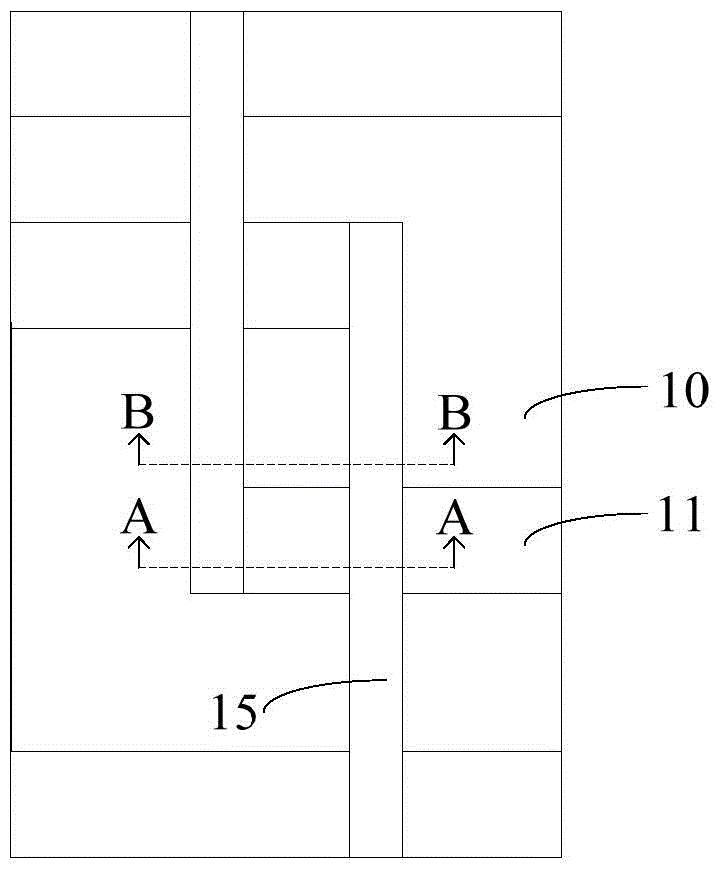
[0052] combined reference Figure 7 and Figure 8 , providing a semiconductor substrate including an active region 31 and an isolation region 30 adjacent to the active region 31 .

[0053] In this embodiment, the semiconductor substrate is a silicon substrate. In other embodiments, the semiconductor substrate can also be a germanium silicon substrate, a III-V group element compound substrate, a silicon carbide substrate or its stacked structure, or a diamond substrate, or other semiconductor materials known to those skilled in the art substrate.

[0054] Wherein, the material of the isolation region 30 is silicon oxide. The methods for forming the active region 31 and the isolation region 30 are well known to those skilled in the art and will not be repeated here.

[0055] Next, a gate structure 32 is formed on the semiconductor substrate, and the gate structure 32 straddles the active region 31 and the isolation region 30 .

[0056] In this embodiment, the active region ...

Embodiment 2

[0119] This embodiment provides a method for forming a transistor, the difference from Embodiment 1 is:

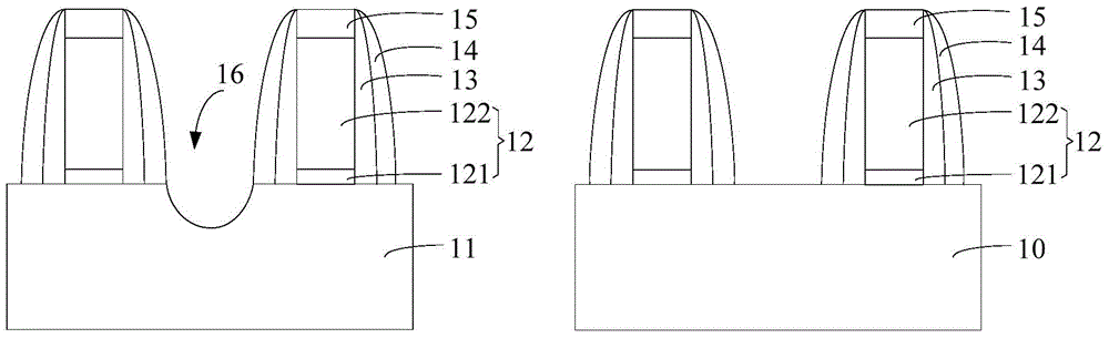
[0120] After the step of forming the first sidewall and before the step of forming the first groove, the step of performing ion implantation on the isolation region, the first sidewall, the patterned mask layer and the active region to form a protection layer. In this way, a protection layer is formed simultaneously in the active region and the isolation region between the gate structures.

[0121] Next, using the first sidewall as a mask, the active region between the gate structures is etched to form a first groove. Afterwards, when the silicon oxide on the surface of the first groove is removed by hydrofluoric acid cleaning, the protective layer formed at the isolation region will prevent the isolation region from being corroded by hydrofluoric acid. After that, continue to etch the first groove to form the second groove. Correspondingly, when the silicon oxide on the...

Embodiment 3

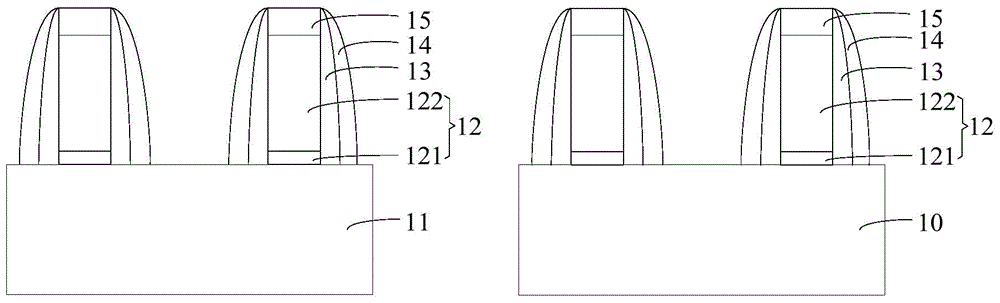
[0125] refer to Figure 14 , the present embodiment provides a transistor, including: a semiconductor substrate, the semiconductor substrate includes an active region 31 and an isolation region 30 adjacent to the active region;

[0126] a gate structure 32 located on the semiconductor substrate and across the active region 31 and the isolation region 30 adjacent to the active region;

[0127] a second side wall 35 located around the gate structure 32, a third side wall 41 located around the second side wall;

[0128] The common source or common drain located between adjacent third sidewalls 41 is characterized in that the semiconductor substrate further includes:

[0129] The protection layer 37 is located on the surface of the isolation region 30 .

[0130] The protection layer 37 is a silicon ion implantation layer.

[0131] In other embodiments, not forming at least one of the second side wall or the third side wall also falls within the protection scope of the present i...


PUM


Abstract

The invention discloses an MOS transistor and an MOS transistor manufacturing method. The MOS transistor manufacturing method comprises the steps of: providing a semiconductor substrate which comprises an active region and an isolation region adjacent to the active region; forming gate structures on the semiconductor substrate, wherein the gate structures stretch across the active region and the isolation region; forming a first groove in the active region on two sides of the gate structures; forming protective layers on surfaces of the active region and the isolation region on two sides of the gate structures; and cleaning the first groove, and removing an oxide on the surface of the first groove. The MOS transistor manufactured by adopting the manufacturing method provided by the invention has high performance.

Description

technical field [0001] The invention relates to the field of semiconductors, in particular to a manufacturing method of a MOS transistor and the MOS transistor. Background technique [0002] In the existing manufacturing process of semiconductor devices, since stress can change the energy gap and carrier mobility of silicon materials, it has become an increasingly common means to improve the performance of MOS transistors through stress. Specifically, by properly controlling the stress, the mobility of carriers (electrons in NMOS transistors and holes in PMOS transistors) can be increased, thereby increasing the driving current, thereby greatly improving the performance of MOS transistors. For PMOS transistors, embedded silicon germanium technology (Embedded SiGe Technology) can be used to generate compressive stress in the channel region of the transistor, thereby improving carrier mobility. The so-called embedded silicon germanium technology refers to burying silicon germ...

Claims


Application Information

Patent Timeline
Patent Type & Authority Applications(China)
IPC IPC(8): H01L21/336H01L29/78H01L29/06
Inventor 刘佳磊
Owner SEMICON MFG INT (SHANGHAI) CORP
Why Eureka
Try Eureka