Silicon-based photoelectrode and preparation method and application thereof

A photoelectrode, silicon-based technology, applied in electrodes, electrolysis process, electrolysis components, etc., can solve the problems of low catalytic efficiency and poor electrochemical activity, achieve high electrocatalytic activity, improve electrocatalytic activity, and high controllability Effect

Active Publication Date: 2019-06-28
THE NAT CENT FOR NANOSCI & TECH NCNST OF CHINA
View PDF3 Cites 5 Cited by
  • Summary
  • Abstract
  • Description
  • Claims
  • Application Information

AI Technical Summary

Problems solved by technology

The Ni / n-Si photoanode photoelectrochemical water splitting onset potential method is simple to operate and low in cost, but its electrochemical activity is poor and its catalytic efficiency is low

Method used


Image

  • Silicon-based photoelectrode and preparation method and application thereof
  • Silicon-based photoelectrode and preparation method and application thereof
  • Silicon-based photoelectrode and preparation method and application thereof

Examples


Embodiment 1

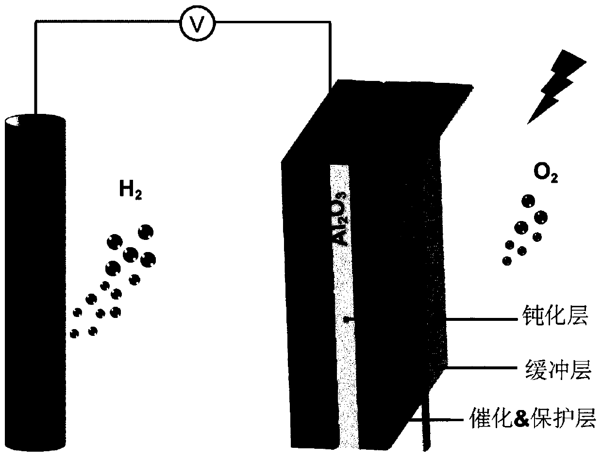
[0069] A method for preparing a silicon-based photoelectrode comprises the steps of:

[0070] (1) Ultrasonic cleaning of a 1 cm × 1 cm Si wafer in acetone, isopropanol and deionized water three times for 5 minutes each time, followed by drying with nitrogen, and soaking the dried silicon wafer in 3% HF solution 2 minutes to remove the natural oxide layer on the surface of the silicon wafer, then rinse repeatedly with deionized water to clean the residual HF on the surface, and blow dry with nitrogen;

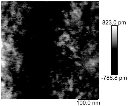
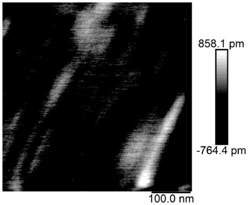
[0071] (2) Using trimethylaluminum as Al precursor, deionized water as oxygen source, N 2 As a carrier gas, the sample is first evacuated to a vacuum at a pressure of about 0.2 Pa, and then the HF etched Si substrate is heated to 200°C. Each cycle of ALD includes a 15ms trimethylaluminum pulse and a 15s nitrogen purge. , 15ms deionized water pulse and 15s nitrogen purge, cycle 25 circles to obtain a passivation layer with a thickness of 2.2nm, the passivation layer is Al 2 o ...

Embodiment 2

[0075] The difference from Example 1 is that in step (4), a nickel-iron alloy with a nickel:iron atomic ratio of 9:1 is used as the target material, and the iron content in the catalytic protective layer is 5.79%.

Embodiment 3

[0077] The difference from Example 1 is that in step (4), a nickel-iron alloy with a nickel:iron atomic ratio of 2:1 is used as the target material, and the iron content in the catalytic protective layer is 9.02%.


PUM

PropertyMeasurementUnit
thicknessaaaaaaaaaa
thicknessaaaaaaaaaa
thicknessaaaaaaaaaa

Abstract

The invention relates to a silicon-based photoelectrode and a preparation method and application thereof. The silicon-based photoelectrode includes a Si layer, a passivation layer, a buffer layer anda catalytic protection layer, wherein the passivation layer, the buffer layer and the catalytic protection layer are sequentially disposed on the surface of the Si layer. The passivation layer, the buffer layer and the catalytic protection layer in the silicon-based photoelectrode are all made of dense film materials, wherein the catalytic protection layer has high electrocatalytic activity and can effectively reduce the reaction overpotential and maintain high stability in a solution; the passivation layer on the surface of the Si layer can reduce the surface state of Si, reduce Fermi level pinning and inhibit the recombination of electrons and holes on the silicon surface; the buffer layer can protect the passivation layer from damage in the process of preparing the catalytic protectionlayer, and the photoelectric property of the photoelectrode is improved from two aspects including thermodynamics and kinetics.

Description

technical field [0001] The invention belongs to the field of photoelectric catalysis, and in particular relates to a silicon-based photoelectrode, its preparation method and application. Background technique [0002] Photoelectrochemical water splitting is one of the effective ways to convert solar energy into clean energy and solve energy crisis and environmental pollution. Photoelectrochemical water splitting involves two half-reactions: the reduction of water at the cathode to produce hydrogen, and the oxidation of water at the anode to produce oxygen. Compared with the reduction reaction, the oxygen evolution reaction involving a four-electron transfer process faces more severe challenges due to its slow kinetics and high overpotential. Therefore, it is crucial to design a stable and efficient photoanode for usable solar water splitting. [0003] As a good photoanode material, n-Si has attracted extensive attention of researchers in recent years. Si not only has abund...

Claims


Application Information

Patent Timeline
Patent Type & Authority Applications(China)
IPC IPC(8): C25B1/04C25B11/06C23C16/455C23C16/40C23C16/02C23C14/24C23C14/16C23C14/08C22C19/03C23C14/35C23C28/00
CPCY02E60/36Y02P20/133
Inventor 赵唱郭北斗宫建茹
Owner THE NAT CENT FOR NANOSCI & TECH NCNST OF CHINA
Why Eureka
Try Eureka