A trench Schottky barrier diode and method of making the same

A Schottky potential and diode technology, which is applied in semiconductor/solid-state device manufacturing, electrical components, circuits, etc. wear and other problems, to improve the forward conduction characteristics, reduce reverse leakage, and high reverse blocking voltage.

Active Publication Date: 2018-04-17
HANGZHOU LION MICROELECTRONICS CO LTD
View PDF5 Cites 0 Cited by
  • Summary
  • Abstract
  • Description
  • Claims
  • Application Information

AI Technical Summary

Problems solved by technology

When the device is reverse biased, the maximum electric field intensity inside the device is located on the top surface of the N-type epitaxial layer near the barrier interface; at the same time, there is also a barrier height reduction effect, that is, as the reverse bias voltage increases, the barrier height reduced phenomenon
The above two points make the reverse leakage of the device increase rapidly with the increase of the reverse bias voltage, and eventually cause the device to break down, which seriously limits the performance and device reliability of the planar Schottky barrier diode

Method used


Image

  • A trench Schottky barrier diode and method of making the same
  • A trench Schottky barrier diode and method of making the same
  • A trench Schottky barrier diode and method of making the same

Examples


Embodiment 1

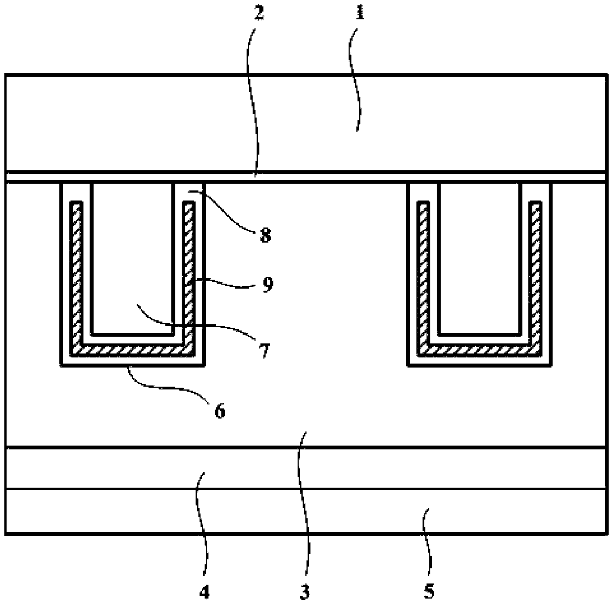
[0048] Such as figure 1 As shown, a trench Schottky barrier diode includes an active region in the middle and a cut-off region surrounding the active region. The active region consists of an anode metal layer 1 and a Schottky barrier metal layer from top to bottom. 2. An N-type lightly doped N-type epitaxial layer 3 of the first conductivity type, a heavily doped monocrystalline silicon substrate 4 of the first conductivity type, and a cathode metal layer 5; several grooves 6 are provided on the upper part of the N-type epitaxial layer , the grooves 6 are arranged laterally at intervals; the Schottky barrier metal layer 2 forms a Schottky barrier contact with the top surface of the N-type epitaxial layer 3 between adjacent grooves; the grooves 6 are filled with conductive polysilicon 7, The top surface of the conductive polysilicon 7 forms an ohmic contact with the Schottky barrier metal layer 2; an isolation layer 8 is provided between the conductive polysilicon 7 and the tre...

Embodiment 2

[0068] The structure of the trench Schottky barrier diode in this embodiment is the same as that in Embodiment 1, except that the width of the vacuum gap 9 in this embodiment is 200 Å, and the vacuum degree of the vacuum gap 9 is 10 Å. -3 Torr, the thickness of Schottky barrier metal layer 2 is 1000Å;

[0069] The manufacturing method of the trench Schottky barrier diode in this embodiment is the same as that in Embodiment 1.

Embodiment 3

[0071] The structure of the trench Schottky barrier diode in this embodiment is the same as that in Embodiment 1, except that the width of the vacuum gap 9 in this embodiment is 1000 Å, and the vacuum degree of the vacuum gap 9 is 10 Å. -6 Torr, the thickness of Schottky barrier metal layer 2 is 5000Å;

[0072] The manufacturing method of the trench Schottky barrier diode in this embodiment is the same as that in Embodiment 1.


PUM


Abstract

The invention discloses a trench Schottky barrier diode. The trench Schottky barrier diode comprises an active region and a cut-off region, wherein the active region consists of a positive electrode metal layer, a Schottky barrier metal layer, a first conduction type lightly-doped N-type epitaxial layer, a first conduction type heavily-doped single crystal silicon substrate and a negative electrode metal layer from top to bottom in sequence; an upper part of the N-type epitaxial layer is provided with a plurality of trenches; the trenches are formed transversely at intervals; the Schottky barrier metal layer is in Schottky barrier contact with a top surface of the N-type epitaxial layer between adjacent trenches; the trenches are filled with conductive polycrystalline silicon; an isolation layer is arranged between the conductive polycrystalline silicon and the trenches; vacuum air gaps are formed inside the isolation layer; and the trenches are communicated in the active region and the cut-off region. The trench Schottky barrier diode has the advantages of high reverse blocking voltage, low reverse bias voltage, low reverse leakage current and the like. The invention also discloses a manufacturing method of the trench Schottky barrier diode. The manufacturing method has the advantages of less steps, low manufacturing cost and the like.

Description

technical field [0001] The invention belongs to the technical field of semiconductors, and in particular relates to a trench Schottky barrier diode and a manufacturing method thereof. Background technique [0002] Schottky barrier diodes are manufactured using the principle of a metal-semiconductor junction formed by contact between a metal and a semiconductor. Traditional planar Schottky barrier diode devices are usually composed of an N-type epitaxial layer with a low doping concentration and a metal layer deposited on the top surface to form a Schottky barrier contact. The work function difference between the metal and N-type single crystal silicon forms a potential barrier, and the height of the potential barrier determines the characteristics of the Schottky barrier diode. The lower barrier height makes the reverse blocking voltage of the device low, the reverse leakage is large, and the forward conduction voltage is reduced; the higher barrier height makes the device ...

Claims


Application Information

Patent Timeline
Patent Type & Authority Patents(China)
IPC IPC(8): H01L29/872H01L21/329H01L29/06
CPCH01L29/06H01L29/0607H01L29/66143H01L29/872H01L29/8725
Inventor 刘伟
Owner HANGZHOU LION MICROELECTRONICS CO LTD
Why Eureka
Try Eureka