

Thin film transistor array and image display device
A technology of thin film transistors and arrays, applied in the field of thin film transistor arrays and image display devices, capable of solving problems such as production volume or cost
- Summary
- Abstract
- Description
- Claims
- Application Information
AI Technical Summary
Problems solved by technology
Method used
Image

Examples
Embodiment 1
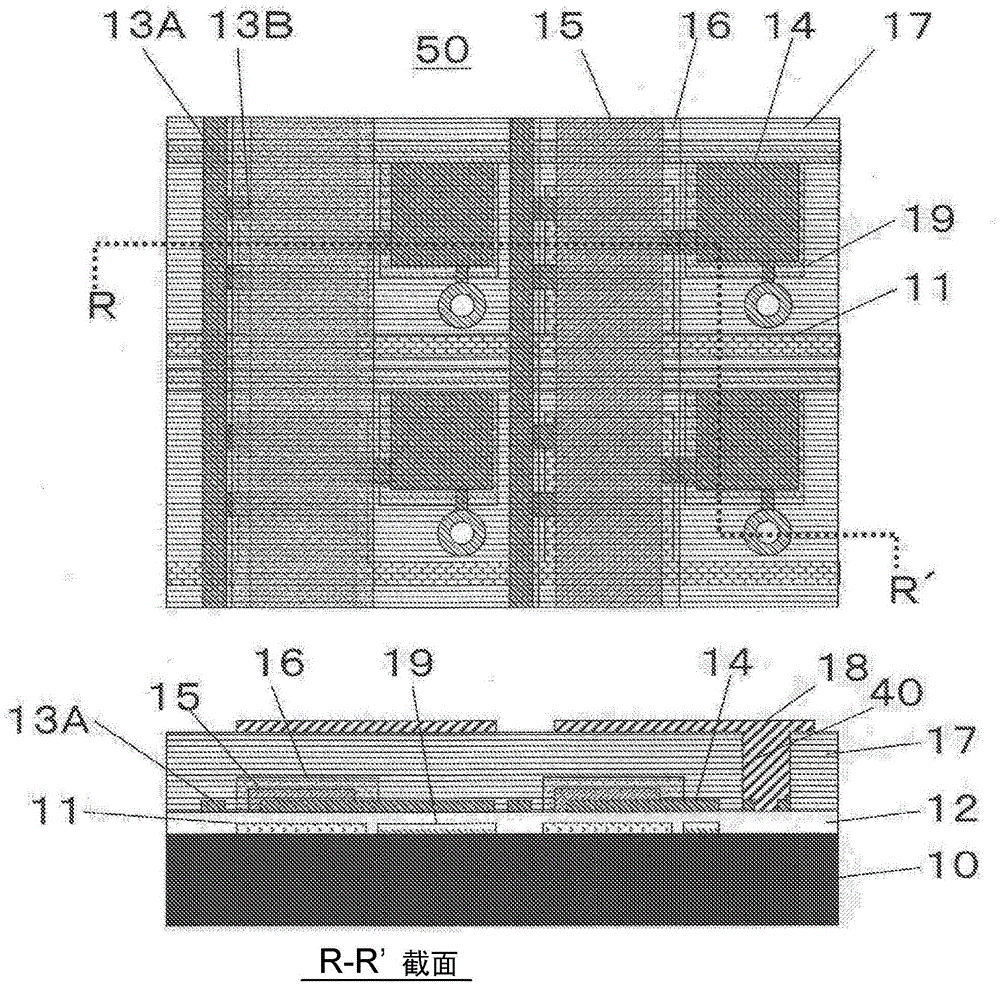
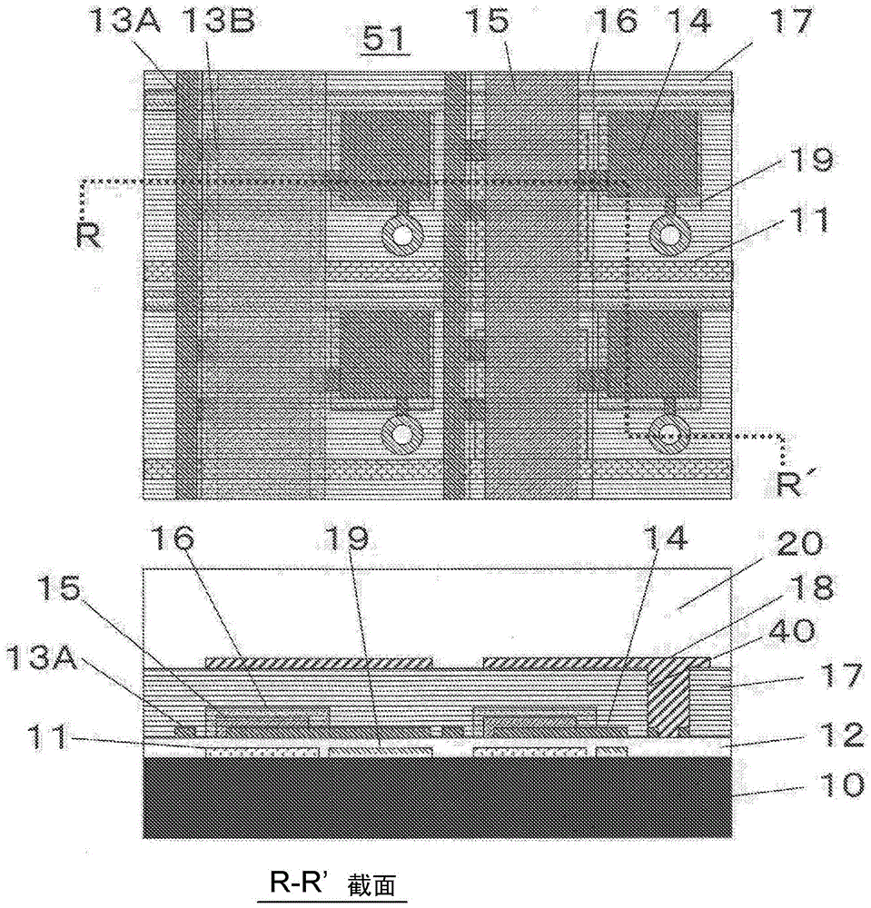
[0048] figure 2 A pattern layout plan view and a cross-sectional structure showing a schematic configuration of the thin film transistor array 51 composed of the bottom-gate bottom-contact type flexible thin film transistor array of the first embodiment are shown. Refer to the following figure 2 The manufacturing method will be described. The size of one element of the thin film transistor array 51 is 300 μm×300 μm, and there are 240×320 elements.
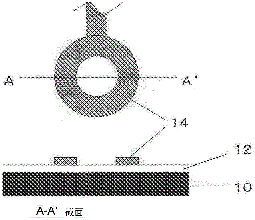
[0049] A polyethylene naphthalate (PEN) film was used as the plastic substrate 10 . After forming a film of 100 nm of aluminum on the PEN film by sputtering, photolithography and etching were performed using a positive resist, and then the resist was peeled off to form gate electrode 11 and capacitor electrode 19 .
[0050] Next, after coating a coating-type photosensitive insulating material (AH series, manufactured by Hitachi Chemical Co., Ltd.) as a gate insulating material by spin coating, the terminal portion of the gate ...
PUM
| Property | Measurement | Unit |
|---|---|---|
| Thickness | aaaaa | aaaaa |
Abstract
Description
Claims
Application Information