Self-aligned two-dimensional crystal material field-effect semiconductor device and preparation method thereof

A two-dimensional crystal and self-alignment technology, which is applied in semiconductor/solid-state device manufacturing, semiconductor devices, transistors, etc., can solve the problems of low switching and difficult application of integrated circuits, so as to reduce covering capacitance, reduce parasitic resistance, and avoid The effect of destruction

Inactive Publication Date: 2016-05-25
UNIV OF ELECTRONICS SCI & TECH OF CHINA
View PDF4 Cites 5 Cited by
  • Summary
  • Abstract
  • Description
  • Claims
  • Application Information

AI Technical Summary

Problems solved by technology

The main problem of graphene is that the band gap is zero, and the switching ratio of semiconductor devices based on graphene materials is relatively low, which makes it difficult to apply in integrated circuits.

Method used


Image

  • Self-aligned two-dimensional crystal material field-effect semiconductor device and preparation method thereof
  • Self-aligned two-dimensional crystal material field-effect semiconductor device and preparation method thereof
  • Self-aligned two-dimensional crystal material field-effect semiconductor device and preparation method thereof

Examples


Embodiment Construction

[0084] The method for preparing a self-aligned two-dimensional crystal material field-effect semiconductor device of the present invention comprises the following steps:

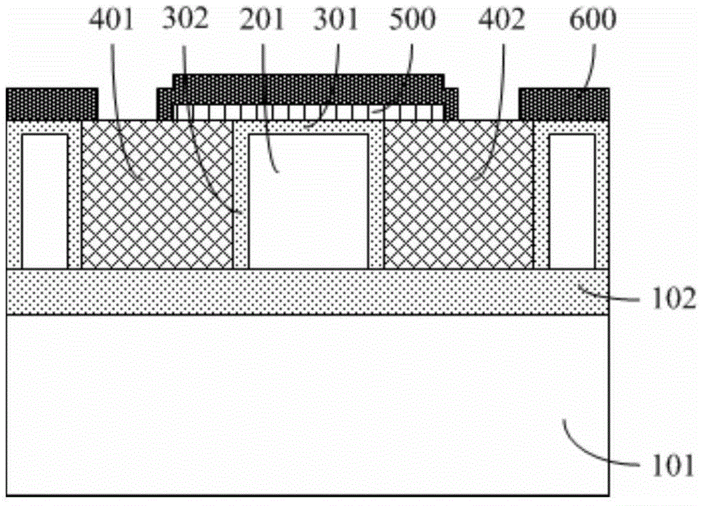
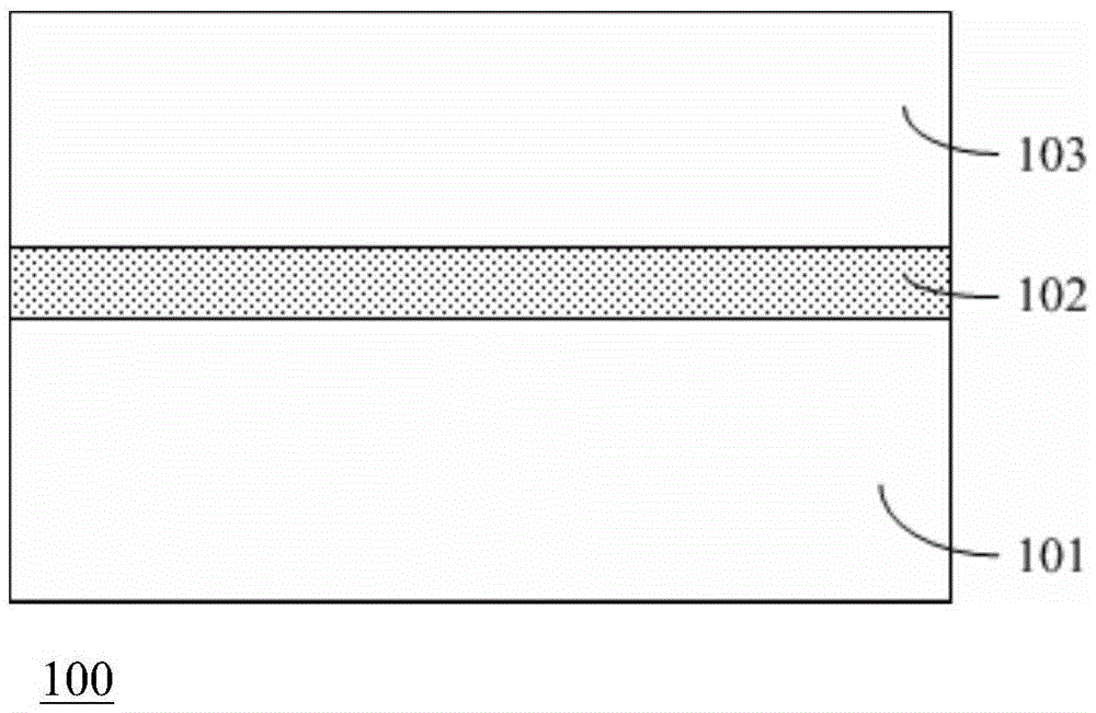
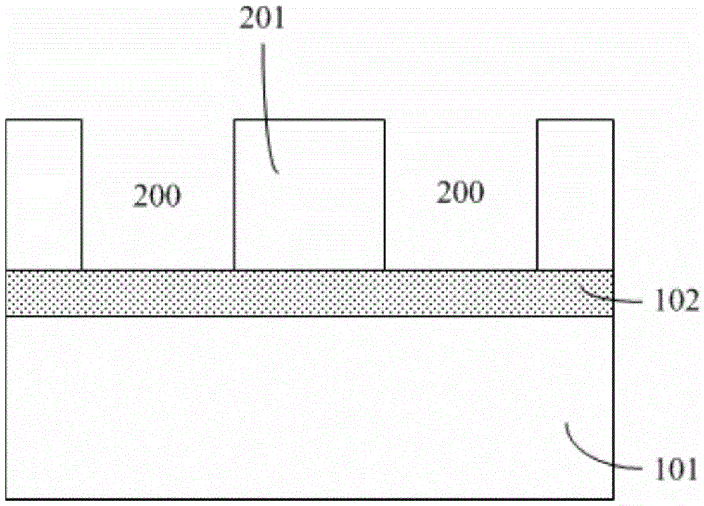
[0085] (1) Select a silicon (SOI) wafer on an insulating substrate as the base, select a suitable mask as a mask, etch the top silicon of the SOI until the buried oxide layer in the SOI is exposed, and the rest after etching The silicon on top of the SOI is the gate electrode of the device.

[0086] (2) Form a layer of good-quality silicon dioxide dielectric on the upper surface and side surfaces of the silicon gate electrode on the top layer of SOI.

[0087] (3) Depositing metal on the surface of the SOI substrate, the thickness of the metal layer is greater than the depth of the existing grooves on the surface of the SOI substrate.

[0088] (4) The metal layer is planarized by using a planarization process, and the process is controlled so that the silicon dioxide on the upper surface of the silicon gate ...


PUM


Abstract

The invention provides a self-aligned two-dimensional crystal material field-effect semiconductor device and a preparation method thereof, and belongs to the technical field of semiconductor devices. The semiconductor device provided by the invention comprises a gate electrode region, a source electrode region, a drain electrode region and a two-dimensional crystal material layer, wherein the two-dimensional crystal material layer is connected with a source electrode and a drain electrode, and strides the local part of the gate electrode region; and a gate dielectric oxidation layer is arranged between the two-dimensional crystal material layer and the gate electrode region at the lower part of the two-dimensional crystal material layer. By a self-aligned technology provided by the invention, position alignment of the gate electrode and the source electrode and the drain electrode of the device can be automatically achieved, so that, on one hand, the coverage capacitance of the gate electrode, the source electrode and the drain electrode is greatly reduced, which has important significance for improvement of the working frequency of the device; and on the other hand, the self-aligned device structure with the gate electrode, the source electrode and the drain electrode greatly reduces channel layers, namely the parasitic resistance of the two-dimensional crystal material, between the gate electrode and the source electrode and between the gate electrode and the drain electrode, which is also beneficial to improvement of the working frequency of the device.

Description

technical field [0001] The invention relates to a self-aligned two-dimensional crystal material-based field-effect semiconductor device structure and a preparation method thereof, belonging to the technical field of semiconductor devices. Background technique [0002] Driven by Moore's Law, the size of semiconductor devices based on single crystal silicon materials is getting smaller and smaller, the density of integrated circuits is getting higher and higher, power consumption is getting lower and lower, the performance of chips is getting stronger, and the cost is getting lower and higher. Low. However, with the gradual reduction of the critical dimensions of the semiconductor process, the semiconductor process is getting closer and closer to the physical limit of the semiconductor, and it is difficult to continue shrinking. [0003] Moore's Law is coming to an end, but the pace of information technology advancement will not slow down. Researchers from all over the world...

Claims


Application Information

Patent Timeline
Patent Type & Authority Applications(China)
IPC IPC(8): H01L29/04H01L29/10H01L29/78H01L21/336H01L21/34
CPCH01L29/04H01L29/1033H01L29/66045H01L29/66575H01L29/66969H01L29/78
Inventor 王刚李平张庆伟
Owner UNIV OF ELECTRONICS SCI & TECH OF CHINA
Why Eureka
Try Eureka