Step-down circuit in medium voltage and high voltage integrated circuit

An integrated circuit and step-down circuit technology, applied in electrical components, output power conversion devices, etc., can solve the problems of large static current, high resource consumption, complex circuit structure and process of the conversion circuit, and achieve low static current consumption, Simple circuit structure, good effect of step-down and voltage regulation

Inactive Publication Date: 2016-06-08
TAIZHOU SUB CORE MICROELECTRONICS TECH CO LTD
View PDF3 Cites 5 Cited by
  • Summary
  • Abstract
  • Description
  • Claims
  • Application Information

AI Technical Summary

Problems solved by technology

The advantage of this method is that the output voltage is more accurate, but its disadvantages are obvious: the quiescent current consumed by the conversion circuit is relatively large, the circuit structure and process are complex, the resource consumption is high, and a relatively complicated resistance correction process is required during mass production.

Method used


Image

  • Step-down circuit in medium voltage and high voltage integrated circuit
  • Step-down circuit in medium voltage and high voltage integrated circuit

Examples


no. 1 example

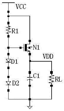
[0012] The first embodiment: a step-down circuit in a medium-high voltage integrated circuit, which includes a MOS transistor N1 and a capacitor C1. It is characterized in that the drain of the MOS transistor N1 is connected to the input terminal VCC of the high-voltage power supply for external power supply, and the source of the MOS transistor N1 The pole is grounded through the capacitor C1, the source of the MOS transistor N1 is the output terminal VDD of the low-voltage power supply to supply power to the internal control circuit part, the substrate of the MOS transistor N1 is grounded, and the gate of the MOS transistor N1 is connected to a control voltage signal. The MOS tube is a high-voltage N-channel consumption or zero-volt intrinsic tube. The control voltage signal is generated by a circuit composed of resistor R1, diode D1, and D2. One end of resistor R1 is connected to the input terminal VCC of the high-voltage power supply, and The other end is connected to the a...

no. 2 example

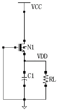
[0020] The second embodiment: when the turn-on voltage Vth of the MOS transistor N1 reaches a more negative voltage (such as -1.5v), within the voltage range of the output terminal VDD, the diode and resistor can be omitted, that is, the gate of the MOS transistor N1 Directly grounded, since there is no diode, the influence of temperature on the whole circuit is almost negligible, and the circuit will become simpler and more reliable.

[0021] It should be noted that, in the current integrated circuit technology, whether it is high voltage or low voltage, the power dissipation device has become one of the commonly used devices. Of course, there are also some low-voltage processes that only provide zero turn-on voltage intrinsic transistors (NativeMOS), which can also be used by using the working principle of this circuit.


PUM


Abstract

A step-down circuit in a medium voltage and high voltage integrated circuit provides a power source for a low-voltage control part in the integrated circuit. The step-down circuit comprises an MOS transistor N1 and a capacitor C1 and is characterized in that a drain electrode of the MOS transistor N1 is connected with an input end VCC of an external power-supply high-voltage power source, a source electrode of the MOS transistor N1 is grounded through the capacitor C1, the source electrode of the MOS transistor N1 is connected with an output end VDD of a low-voltage power source and supplies power to an inner control circuit, a substrate of the MOS transistor N1 is grounded, a grid electrode of the MOS transistor N1 is connected with a control voltage through signals, the MOS transistor is a high-voltage type N-channel depletion transistor or a zero-voltage intrinsic transistor, and the voltage value of a control voltage signal is larger than or equal to 0V. The step-down circuit is simple in structure and reliable, static current consumption is small, and step-down performance and voltage stabilizing performance are good.

Description

technical field [0001] The invention relates to a step-down circuit in a medium and high voltage integrated circuit, which can convert the medium and high voltage power supply supplying power to the integrated circuit into a low voltage power supply inside the integrated circuit. This circuit can be widely used in high and low voltage mixed circuits with internal logic control Power management circuits, digital-analog hybrid circuits, etc. Background technique [0002] The application of high-voltage integrated circuits is becoming more and more extensive, and has been widely used in LED drivers, adapters, electrical control and other occasions. The high-voltage circuit with intelligent control is developing rapidly and is more and more favored by people. Medium and high-voltage integrated circuits generally have a high power supply voltage, usually above 7V, which is difficult to directly provide to the intelligent control logic circuit (generally 1.5~5.5v). Although the ...

Claims


Application Information

Patent Timeline
Patent Type & Authority Applications(China)
IPC IPC(8): H02M1/08
CPCH02M1/08
Inventor 唐伟李曙生周国付
Owner TAIZHOU SUB CORE MICROELECTRONICS TECH CO LTD
Why Eureka
Try Eureka