Supercharge Your Innovation With Domain-Expert AI Agents!

A method of electroless copper deposition using pre-contact function and its application device

A technology of electroless copper deposition and pre-contact, which is applied in liquid chemical plating, coating, printed circuit manufacturing, etc., can solve the problem of poor copper deposition rate PCB board copper layer coverage, large fluctuations in resin area of ​​electroless copper deposition rate, and The problem of slow start of the electroless copper deposition process has achieved the effect of strong promotion significance, stable thickness and backlight quality, and high production efficiency

Active Publication Date: 2018-12-04
DONGGUAN MEADVILLE CIRCUITS
View PDF4 Cites 0 Cited by
  • Summary
  • Abstract
  • Description
  • Claims
  • Application Information

AI Technical Summary

Problems solved by technology

[0003] At present, in the relatively common vertical electroless copper deposition process, the chemical solution system used mainly includes the ionic activated palladium catalytic system. However, there are many deficiencies in the existing production process of the ionic activated catalytic solution system. The start is slow, and the chemical copper sinking rate fluctuates greatly with the resin area of ​​the PCB board. The smaller the resin area, the slower the copper sinking speed; and the instability of the copper sinking rate will result in poor coverage of the copper sinking layer of the PCB board, and the sinking copper hole is broken. The risk is high; on the other hand, the use of pure resin boards for co-production in the electroless copper process will result in a decrease in production efficiency

Method used


Image

  • A method of electroless copper deposition using pre-contact function and its application device

Examples


Embodiment Construction

[0018] In order to make the object, technical solution and advantages of the present invention clearer, the present invention will be further described in detail below in conjunction with the accompanying drawings and embodiments.

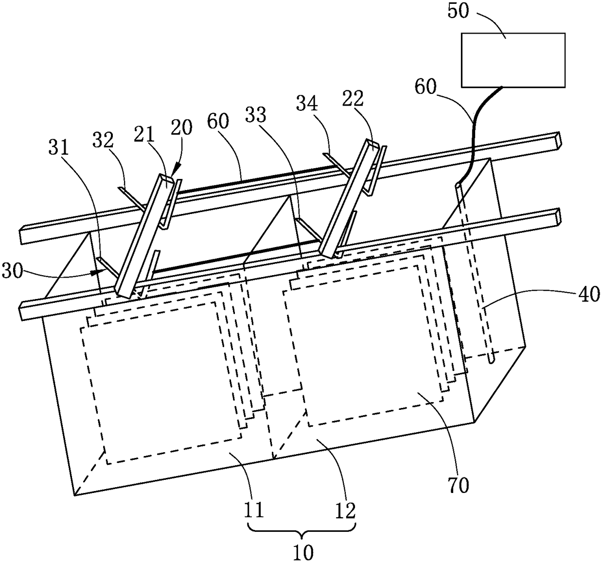
[0019] Such as figure 1 As shown, the present invention provides a PCB chemical deposition copper device, which is used in the PCB electroplating process. machine 50, the positioning seat 30 is arranged on the sinking copper cylinder 10, and the sinking copper cylinder 10 is provided with two oppositely arranged positioning seats 30, and the flying bus 20 is erected on the two positioning seats 30 , the copper immersion cylinder 10 is filled with chemical liquid, the metal titanium rod 40 is placed in the chemical liquid, and is electrically connected to the ballast 50 through a wire 60 .

[0020] The PCB electroless copper deposition device also includes a control terminal, and the ballast 50 is electrically connected to the control terminal. In ...


PUM


Abstract

A PCB electroless plating copper device comprises electroless plating copper vats, conductive bars, locating seats, a metallic titanium bar and a ballast machine; the locating seats are arranged on the electroless plating copper vats, each electroless plating copper vat is provided with two oppositely arranged locating seats, each conductive bar is erected on the two corresponding locating seats, chemical liquid is contained in the electroless plating copper vats, and the metallic titanium bar is placed in the chemical liquid and electrically connected to the ballast machine through a wire. The invention further provides an electroless plating copper adopting a pre-contact function. During the time 30-90 seconds before PCBs are put into the electroless plating copper vats, a negative contact voltage is additionally added to the chemical liquid in the electroless plating copper vats, reaction potentials between the PCBs and the chemical liquid are reduced, rapid conducting of a chemical reaction is facilitated, the stability of plating copper rate in the electroless plating copper process is improved, the thickness and backlight quality of plating copper layers are stable, the hole breakage risk is low, the production efficiency is high, the practicability is high, and strong promotion significance is achieved.

Description

technical field [0001] The invention relates to the field of PCB manufacture, in particular to an electroless copper deposition method using a pre-contact function and an application device thereof. Background technique [0002] Eletcroless Plating Copper (Eletcroless Plating Copper), also known as sinking copper or porosity (PTH), is an autocatalytic redox reaction, which is widely used in the production and processing of printed circuit boards with through holes. The process of making parts including pads, vias, solder mask layers, silk screen layers, and sinking copper. Copper sinking technology is widely used in the production and processing of printed circuit boards with through holes. Its main purpose is to deposit a layer of copper on a non-conductive substrate through a series of chemical treatments, and then thicken it through subsequent electroplating methods to make it To achieve the specific thickness of the design. [0003] At present, in the relatively common...

Claims


Application Information

Patent Timeline
Patent Type & Authority Patents(China)
IPC IPC(8): H05K3/18C23C18/38
CPCC23C18/38H05K3/188H05K2203/0104H05K2203/0723
Inventor 汪斌
Owner DONGGUAN MEADVILLE CIRCUITS
Features
  • R&D
  • Intellectual Property
  • Life Sciences
  • Materials
  • Tech Scout
  • Unparalleled Data Quality
  • Higher Quality Content
  • 60% Fewer Hallucinations
Learn More