
Full-color high-resolution micro-display chip based on gallium nitride LEDs and quantum dot technology

A micro-display chip, high-resolution technology, applied in the direction of identification devices, instruments, electrical components, etc., can solve the problems of cost expenditure hindering mass production, commercialization obstacles, etc., to achieve reduced lateral transmission, low cost, good color gamut coverage Effect

Inactive Publication Date: 2016-06-15
深圳市丽格特光电有限公司
View PDF5 Cites 15 Cited by
  • Summary
  • Abstract
  • Description
  • Claims
  • Application Information

AI Technical Summary

Problems solved by technology

[0004] Full-color, yield, and consistency of luminous wavelength are the main problems at present: the monochromatic Micro-array-LED array can be realized by flip-chip packaging and driver IC bonding, while the RGB array needs to be reposted in red, blue, and The green and three-color dies need to embed hundreds of thousands of LED dies. The LED dies have higher requirements for light efficiency, wavelength consistency, and yield. At the same time, the cost of binning is also a technical bottleneck that hinders mass production. obstacles to commercialization

Method used


Image

  • Full-color high-resolution micro-display chip based on gallium nitride LEDs and quantum dot technology

Examples


Embodiment Construction

[0024] In order to make the object, technical solution and advantages of the present invention clearer, the present invention will be further described in detail below in combination with specific embodiments and with reference to the accompanying drawings. It should be understood that these descriptions are exemplary only, and are not intended to limit the scope of the present invention. Also, in the following description, descriptions of well-known structures and techniques are omitted to avoid unnecessarily obscuring the concept of the present invention.

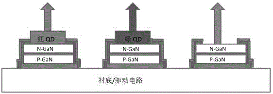
[0025] figure 1 It is a schematic diagram of a pixel structure of a full-color high-resolution microdisplay chip based on gallium nitride LED and quantum dot technology in a preferred embodiment of the present invention,

[0026] Such as figure 1 As shown, a full-color high-resolution microdisplay chip based on gallium nitride LED and quantum dot technology, which uses the light emission of gallium nitride-based LED to ...


PUM

PropertyMeasurementUnit
Heightaaaaaaaaaa

Abstract

The invention relates to the technical field of semiconductor photoelectrons, in particular to a full-color high-resolution micro-display chip based on gallium nitride LEDs and the quantum dot technology.Cadmium selenide (CdSe) quantum dots (QD) of different scales are stimulated by light emitting of the gallium nitride LEDs to generate red, green and blue three radical colors respectively.The chip is composed of the red micron-grade LED capable of independently emitting light, the green micron-grade LED capable of independently emitting light and the blue micron-grade LED capable of independently emitting light.Each stimulated quantum dot is composed of n-Gan and p-Gan, wherein an inverted GaN-based LED is adopted for a Gan-based blue light chip of the stimulated quantum dot, electrodes of the p-GaN are transferred to another substrate through a bonding method, and a drive circuit of pixels is formed on the substrate.The scheme of generating a red, green and blue full-color micro displayer by stimulating the CdSe quantum dots through the GaN blue light chip is adopted, and therefore a better color gamut cover rate, higher color control accuracy and higher red, green and blue color purity are achieved.The advantages of the simple process and low cost are achieved.

Description

technical field [0001] The invention relates to the technical field of semiconductor optoelectronics, in particular to a full-color high-resolution micro-display chip based on gallium nitride LED and quantum dot technology. Background technique [0002] Wearable technology: With the development of Internet +, the rise of the Internet of Things, the development of virtual display (VR) and augmented reality (AR) technologies, wearable electronic products have begun to enter people's production and life. The most representative is Google's "Google Glass". The light-emitting chips used in such glasses have developed from LCD and OLED to array light-emitting diodes (Micro-array-LED). [0003] Micro-array-LED technology refers to the whole array of high-density micro-sized LEDs integrated on a chip. Like an LED display, each pixel can be addressed and individually driven to light up. It can be regarded as a reduced version of an outdoor LED display. The pixel distance is reduced...

Claims


Application Information

Patent Timeline
IPC IPC(8): G09F9/33H01L33/48H01L33/06
CPCG09F9/33H01L33/06H01L33/48
Inventor 刘海明
Owner 深圳市丽格特光电有限公司
Learn More