P-type delafossite structure semiconductor material-based plane structure perovskite solar cell and preparation thereof

A solar cell and planar structure technology, applied in the field of solar cells, can solve problems such as efficiency record growth

Active Publication Date: 2016-06-15
HANGZHOU ZHONGNENG PHOTOELECTRIC TECH CO LTD
View PDF3 Cites 14 Cited by
  • Summary
  • Abstract
  • Description
  • Claims
  • Application Information

AI Technical Summary

Problems solved by technology

Perovskite solar cell technology emerges, albeit short

Method used


Image

  • P-type delafossite structure semiconductor material-based plane structure perovskite solar cell and preparation thereof
  • P-type delafossite structure semiconductor material-based plane structure perovskite solar cell and preparation thereof
  • P-type delafossite structure semiconductor material-based plane structure perovskite solar cell and preparation thereof

Examples


preparation example Construction

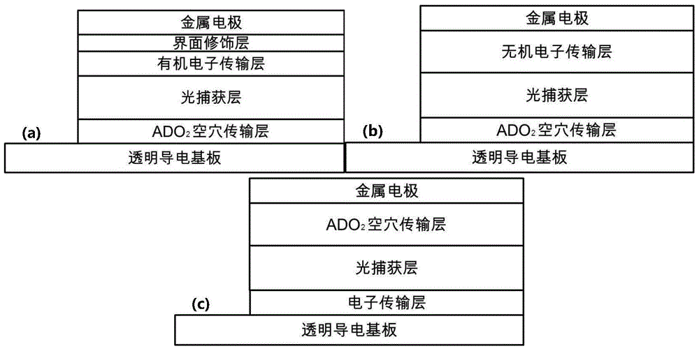
[0051] In one embodiment of the present invention, a kind of preparation method of planar structure perovskite solar cell is provided, such as figure 1 As shown in (a), the solar cell includes a transparent conductive glass substrate or a flexible transparent conductive film substrate, the above-mentioned hole transport layer, the above-mentioned light harvesting layer, an organic electron transport layer, and an interface modification layer from bottom to top And metal electrode, its specific steps are as follows:

[0052] 1) Ultrasonic cleaning of FTO transparent conductive glass or ITO transparent conductive glass or PET flexible transparent conductive film or PI flexible transparent conductive film with deionized water, ethanol and acetone in sequence, and then treated with ultraviolet ozone to obtain a clean substrate;

[0053] 2) in step 1) spin coating or spraying or scraping described ADO on the clean substrate surface 2 The precursor solution of type semiconductor ma...

Embodiment 1a

[0077] Such as figure 1 Shown in (a), the first kind of planar structure perovskite solar cell involved in the present invention consists of substrate (FTO conductive glass or ITO conductive glass or PET flexible transparent conductive film or PI flexible transparent conductive film), CuGaO 2 It is composed of a hole transport layer, a light harvesting layer, an organic electron transport layer, an interface modification layer and a metal electrode. The specific preparation steps are as follows:

[0078] Step 1) Substrate preparation: ultrasonically clean FTO conductive glass or ITO conductive glass or PET flexible transparent conductive film or PI flexible transparent conductive film with deionized water, ethanol and acetone in sequence, and then treat with ultraviolet and ozone for 15 to 30 minutes to obtain Substrate, spare.

[0079] Step 2) CuGaO 2 Hole-transporting thin films (i.e. CuGaO 2 Hole transport layer) preparation: with CuGaO 2 Nanosheets and ethanol or glyco...

Embodiment 1b

[0085] Such as figure 1 Shown in (b), the second planar structure perovskite solar cell involved in the present invention consists of substrate (FTO conductive glass or ITO conductive glass or PET flexible transparent conductive film or PI flexible transparent conductive film), CuGaO 2 It consists of a hole transport layer, a light harvesting layer, an inorganic electron transport layer and a metal electrode, and the specific preparation steps are as follows:

[0086] Step 1) Substrate preparation: ultrasonically clean FTO conductive glass or ITO conductive glass or PET flexible transparent conductive film or PI flexible transparent conductive film with deionized water, ethanol and acetone in sequence, and then treat with ultraviolet and ozone for 15 to 30 minutes to obtain Substrate, spare.

[0087] Step 2) CuGaO 2 Hole-transporting thin films (i.e. CuGaO 2 Hole transport layer) preparation: with CuGaO 2 Nanosheets and ethanol or glycol ether are used as sources, and the ...


PUM

PropertyMeasurementUnit
Thicknessaaaaaaaaaa
Thicknessaaaaaaaaaa

Abstract

The invention relates to a plane structure perovskite solar cell and a preparation method thereof. The cell comprises a hole transport layer and a light capture layer, wherein the light capture layer is prepared from an MXZ3-type perovskite material; M is selected from Cs<+>, CH3NH3<+>, CH3CH2NH3<+>, CH(NH2)2<+> or a mixture thereof; X is selected from Pb<2+>, Sn<2+>, Ge<2+> or a mixture thereof; Z is selected from Cl<->, Br<->, I<-> or the mixture thereof; the hole transport layer is prepared from a doped or un-doped ADO2-type semiconductor material with a p-type delafossite structure; A is selected from Cu or Ag; D is selected from one or more of Cr, Ga, Sc, In, Y or Fe; and a doping element is selected from one or two of Mg, Ca, Sr or Ga. A film of the hole transport layer provided by the invention has good electrical conductivity, proper energy level position, high transmittance and low cost; a solar cell device with excellent and stable performance can be obtained; and propulsion of industrialization of the perovskite solar cell is facilitated.

Description

technical field [0001] The invention belongs to the technical field of solar cells, relates to a solar cell structure and a preparation method thereof, in particular to ADO with a p-type delafossite structure 2 A planar structure perovskite solar cell with a type semiconductor material as a hole transport layer and a preparation method thereof. Background technique [0002] Solar energy is an inexhaustible renewable clean energy with unique advantages and huge development potential. The large-scale development and utilization of solar energy is of great significance for establishing a reasonable green energy structure and achieving the goal of maximum energy conservation and emission reduction. Currently, the relatively mature photovoltaic technologies in the market include the first-generation silicon-based semiconductor solar cells and the second-generation CIGS, CdTe and other multi-component thin-film solar cells. Although the annual growth rate is 30%, the total instal...

Claims


Application Information

Patent Timeline
IPC IPC(8): H01L51/42H01L51/46H01L51/48
CPCH10K71/12H10K85/141H10K30/10Y02E10/549Y02P70/50
Inventor 石磊徐志立
Owner HANGZHOU ZHONGNENG PHOTOELECTRIC TECH CO LTD
Why Eureka
Try Eureka