Laser-enhanced hydrogen passivation method and application of highly efficient passivation of low-price silicon material defects and impurities
A silicon material and low price technology, applied in the field of laser-enhanced hydrogen passivation for efficient passivation of low-price silicon material defects and impurities, can solve problems such as poor stability, achieve high stability, improve efficiency, and moderate equipment prices
- Summary
- Abstract
- Description
- Claims
- Application Information
AI Technical Summary
Problems solved by technology
Method used
Image

Examples
Embodiment 1
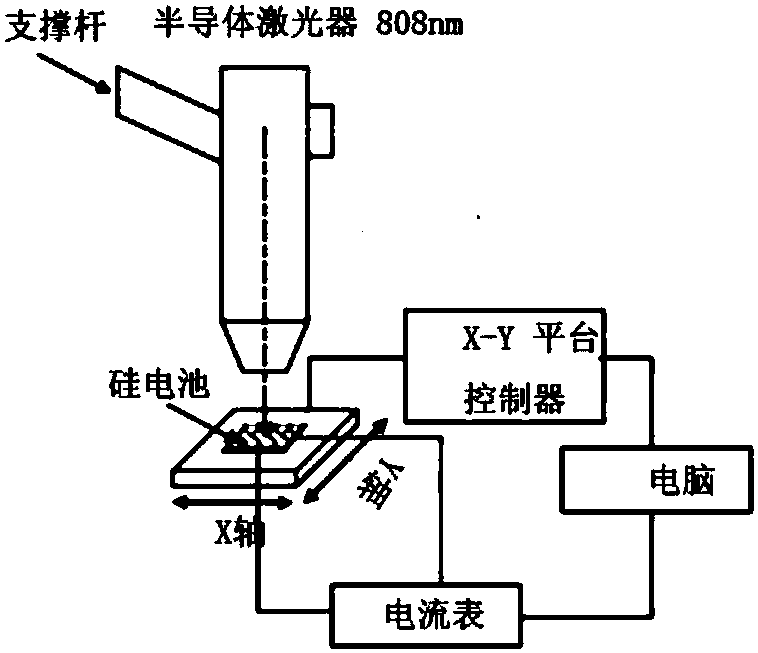
[0033] (1) Pretreatment of low-priced silicon materials: clean the cast-mono silicon materials with RCA solution and 5% HF solution by volume fraction to remove impurities on the surface.
[0034] (2) Use screen printing technology to make low-price silicon cells from pretreated silicon wafers.
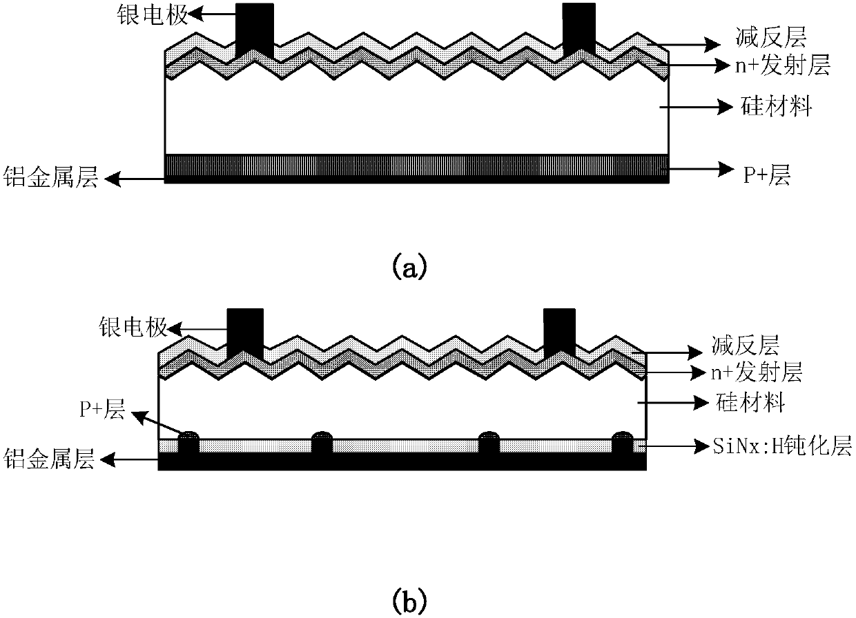
[0035] Diffusion of phosphorus element into the pretreated silicon material in step (1), so that the resistivity on the surface of the silicon material reaches 40-100Ω / □, and an n+ emission layer is formed on the upper surface of the silicon material; using plasma enhanced chemical vapor deposition (PECVD ) grow a layer of 75nm SiNx:H passivation layer on the upper surface of the n+ emission layer of silicon material, and the SiN on the upper surface of the n+ emission layer x The :H passivation layer also acts as an anti-reflection layer; x: The upper surface of the H passivation layer and the lower surface of the silicon material are respectively laid with a silver metal grid and a...
Embodiment 2
[0038] (1) Pretreatment of low-priced silicon materials: the polysilicon materials are cleaned with RCA solution and 5% HF solution by volume fraction to remove impurities on the surface.
[0039] (2) Use screen printing technology to make low-price silicon cells from pretreated silicon wafers.
[0040] Diffusion of phosphorus element into the pretreated silicon material in step (1), so that the resistivity on the surface of the silicon material reaches 40-100Ω / □, and an n+ emission layer is formed on the upper surface of the silicon material; using plasma enhanced chemical vapor deposition (PECVD ) grow a layer of 85nm SiNx on the upper surface of the silicon material n+ emission layer: H passivation layer, the SiN on the n+ emission layer upper surface x The :H passivation layer also acts as an anti-reflection layer; x : The upper surface of the H passivation layer and the lower surface of the silicon material are respectively laid with a silver metal mesh and an aluminum m...
Embodiment 3
[0043] (1) Pretreatment of low-priced silicon materials: UMG silicon materials are cleaned with RCA reagent and 5% HF solution by volume fraction to remove impurities and oxide layers on the surface of low-priced silicon materials;
[0044] (2) Using PERC battery manufacturing technology (see step (2) of the content of the invention for details) to make silicon wafers pretreated in step (1) into low-price silicon batteries:
[0045] Diffusion of phosphorus element into the pretreated silicon material in step (1), so that the resistivity of the silicon material surface reaches 60-100Ω / □, and an n+ emission layer is formed on the upper surface of the silicon material; using plasma enhanced chemical vapor deposition (PECVD ) growing a 75-80nm SiNx:H passivation layer on the upper surface of the n+ emitting layer and the lower surface of the silicon material respectively. SiN on the upper surface of the n+ emitter layer x The :H passivation layer also acts as an anti-reflection l...
PUM
 Abstract
Description
Claims
Application Information
 - R&D
- Intellectual Property
- Life Sciences
- Materials
- Tech Scout
- Unparalleled Data Quality
- Higher Quality Content
- 60% Fewer Hallucinations
Browse by: Latest US Patents, China's latest patents, Technical Efficacy Thesaurus, Application Domain, Technology Topic, Popular Technical Reports.
© 2025 PatSnap. All rights reserved.Legal|Privacy policy|Modern Slavery Act Transparency Statement|Sitemap|About US| Contact US: help@patsnap.com