Preparation method for nitride light emitting diode chip

A technology of light-emitting diodes and nitrides, applied in electrical components, circuits, semiconductor devices, etc., can solve the problems of poor repeatability, complex process, and high control accuracy, and achieve the effects of low cost, improved doping efficiency, and improved luminous efficiency.

Active Publication Date: 2016-06-22
ZHIXIN SEMICON (HANGZHOU) CO LTD
View PDF3 Cites 6 Cited by
  • Summary
  • Abstract
  • Description
  • Claims
  • Application Information

AI Technical Summary

Problems solved by technology

[0004] The technical problem to be solved by the present invention is to provide a method for preparing a nitride light-emitting diode chip, which is a method for preparing a deep ultraviolet light-emitting diode that enhances semiconductor doping efficiency and carrier concentration, and introduces an insulating layer/ The semiconductor structure realizes the semiconductor enhancement effect through the external electric field, and uses the applied voltage to realiz

Method used


Image

  • Preparation method for nitride light emitting diode chip
  • Preparation method for nitride light emitting diode chip
  • Preparation method for nitride light emitting diode chip

Examples


Embodiment 1

[0065] A method for preparing a nitride light-emitting diode chip according to this embodiment, the steps are as follows:

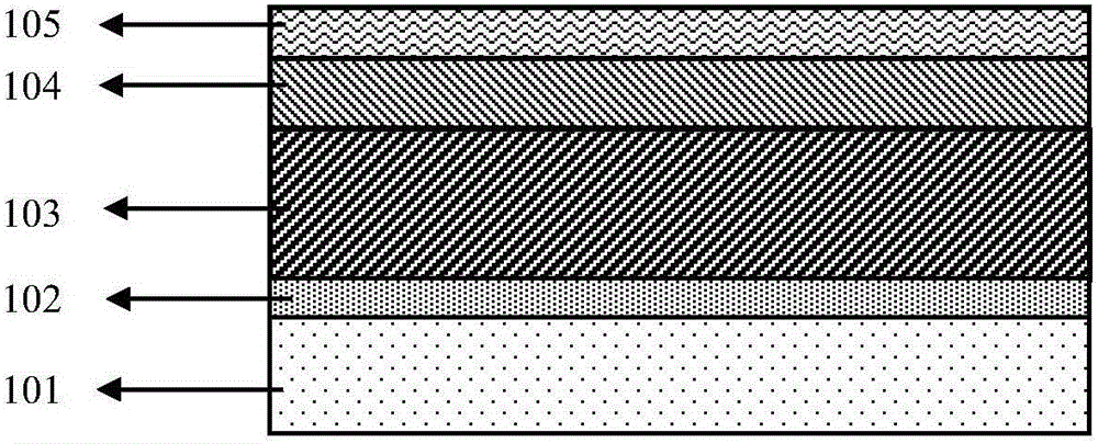
[0066] In the first step, the sapphire substrate 101 is baked at 1200°C in a MOCVD (metal organic compound chemical vapor deposition) reaction furnace to remove foreign matter on the substrate surface;

[0067] In the second step, in the MOCVD reaction furnace, a buffer layer 102 made of AlN with a thickness of 10 nm is epitaxially grown on the surface of the sapphire substrate 101 after the first step;

[0068] In the third step, in the MOCVD reaction furnace, on the buffer layer 102 obtained in the second step, an N-type semiconductor material 103 made of AlN with a thickness of 2 μm is epitaxially grown sequentially, and the material is Al 0.9 Ga 0.1 The thickness of the quantum barrier AlN of N / AlN is 5nm and the quantum well Al 0.9 Ga 0.1 N multi-quantum well layer 104 with a thickness of 1 nm and a P-type semiconductor material 105 made of AlN wi...

Embodiment 2

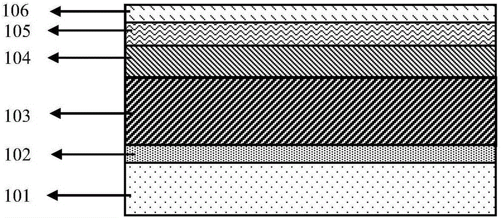
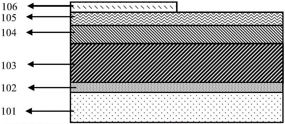
[0076] Except that the substrate 101 is AlN, the material of the current spreading layer 106 is graphene, the insulating layer 107 is LiF, and the position and step pattern of the part of the insulating layer 107 remaining on the step pattern II of the N-type semiconductor material 103 in the sixth step The distance between the sidewalls of II is 50 microns, and the distance between the portion of the insulating layer 107 remaining on the step pattern I on the P-type semiconductor material 105 and the sidewall of the step pattern I is 50 microns, and the others are the same as in Embodiment 1.

Embodiment 3

[0078] Except that the substrate 101 is quartz glass, the material of the current spreading layer 106 is aluminum, the insulating layer 107 is PMMA, and the position and the step pattern of the insulating layer 107 remaining on the step pattern II of the N-type semiconductor material 103 in the sixth step The distance between the sidewalls of II is 100 microns, and the distance between the portion of the insulating layer 107 remaining on the step pattern I on the P-type semiconductor material 105 and the sidewall of the step pattern I is 100 microns, and the others are the same as in Embodiment 1.


PUM

PropertyMeasurementUnit
Thicknessaaaaaaaaaa
Thicknessaaaaaaaaaa
Thicknessaaaaaaaaaa

Abstract

The invention discloses a preparation method for a nitride light emitting diode chip and relates to a semiconductor device which is provided with at least one potential jump barrier or surface barrier and is special for light emission. The preparation method is a preparation method for a deep ultraviolet light emitting diode, which is capable of enhancing the semiconductor doping efficiency and the carrier concentration. An insulating layer/semiconductor structure is introduced into a light emitting diode structure, the semiconductor enhancement effect is realized through an external electric field, band bending is realized by utilizing the impressed voltage to cause increase of the local carrier concentration, so that the doping efficiency is indirectly improved, and the light emitting efficiency of the light emitting diode is finally improved. The preparation method overcomes the defects that the existing technology takes control to increase the doping efficiency of the light emitting diode and the carrier concentration during epitaxial growth and requires high control precision, complex process and poor repeatability.

Description

technical field [0001] The technical solution of the invention relates to a semiconductor device specially suitable for light emission with at least one potential jump barrier or surface barrier, specifically a method for preparing a nitride light-emitting diode chip. Background technique [0002] At present, green energy saving has become a global trend, and III-V nitride semiconductor light-emitting diode technology has been widely used in the fields of display, lighting and backlight due to its characteristics of green environmental protection, high efficiency and energy saving, smart and convenient. In recent years, deep ultraviolet III-V nitride semiconductor light-emitting diodes have also attracted great attention. In the future, deep ultraviolet light-emitting diodes will generate huge economic benefits. However, in the current deep ultraviolet light-emitting diodes, P-type semiconductors and N- The low doping efficiency and carrier concentration of type semiconducto...

Claims


Application Information

Patent Timeline
IPC IPC(8): H01L33/00H01L33/32H01L33/02H01L33/14
CPCH01L33/0075H01L33/02H01L33/14
Inventor 张紫辉张勇辉毕文刚徐庶耿翀
Owner ZHIXIN SEMICON (HANGZHOU) CO LTD
Why Eureka
Try Eureka