A giant piezoresistive double resonance mass sensor and its manufacturing method

A quality sensor and resonant sensor technology, applied in micro-nano electro-mechanical systems, giant piezoresistive double-resonant mass sensors and their production fields, can solve the problem of accuracy, small silicon piezoresistor gauge coefficient, net output voltage limitation, etc. problem, to achieve the effect of improving detection sensitivity and resolution, improving sensitivity and resolution, and improving accuracy

Active Publication Date: 2018-09-14
南京知行慧芯科技有限公司
View PDF7 Cites 0 Cited by
  • Summary
  • Abstract
  • Description
  • Claims
  • Application Information

AI Technical Summary

Problems solved by technology

[0003] However, the current resonant mass sensor has the following problems: (1) In the liquid detection environment, the net output voltage of the sensor electrical signal output terminal is greatly limited under the influence of the electrolyte solution
In addition, due to the effect of fluid damping, its energy consumption will increase, which will eventually lead to too high dynamic resistance, which will affect the accuracy of measurement; (2) The change of piezoresistive resistance is affected by both the external mass (pressure) and the ambient temperature, Especially in ultra-trace detection, the ambient temperature has a greater impact on the results, and the current resonant mass sensors usually lack temperature compensation measures; (3) The gauge coefficient of the traditional silicon piezoresistor through the doping process is small, with the At present, the size of the sensor is getting smaller, and the piezoresistor of the traditional doping process can no longer meet the requirements of modern high-sensitivity detection, especially the requirements of ultra-trace and ultra-fast detection of biochemical pressure sensors.

Method used


Image

  • A giant piezoresistive double resonance mass sensor and its manufacturing method
  • A giant piezoresistive double resonance mass sensor and its manufacturing method
  • A giant piezoresistive double resonance mass sensor and its manufacturing method

Examples


Embodiment Construction

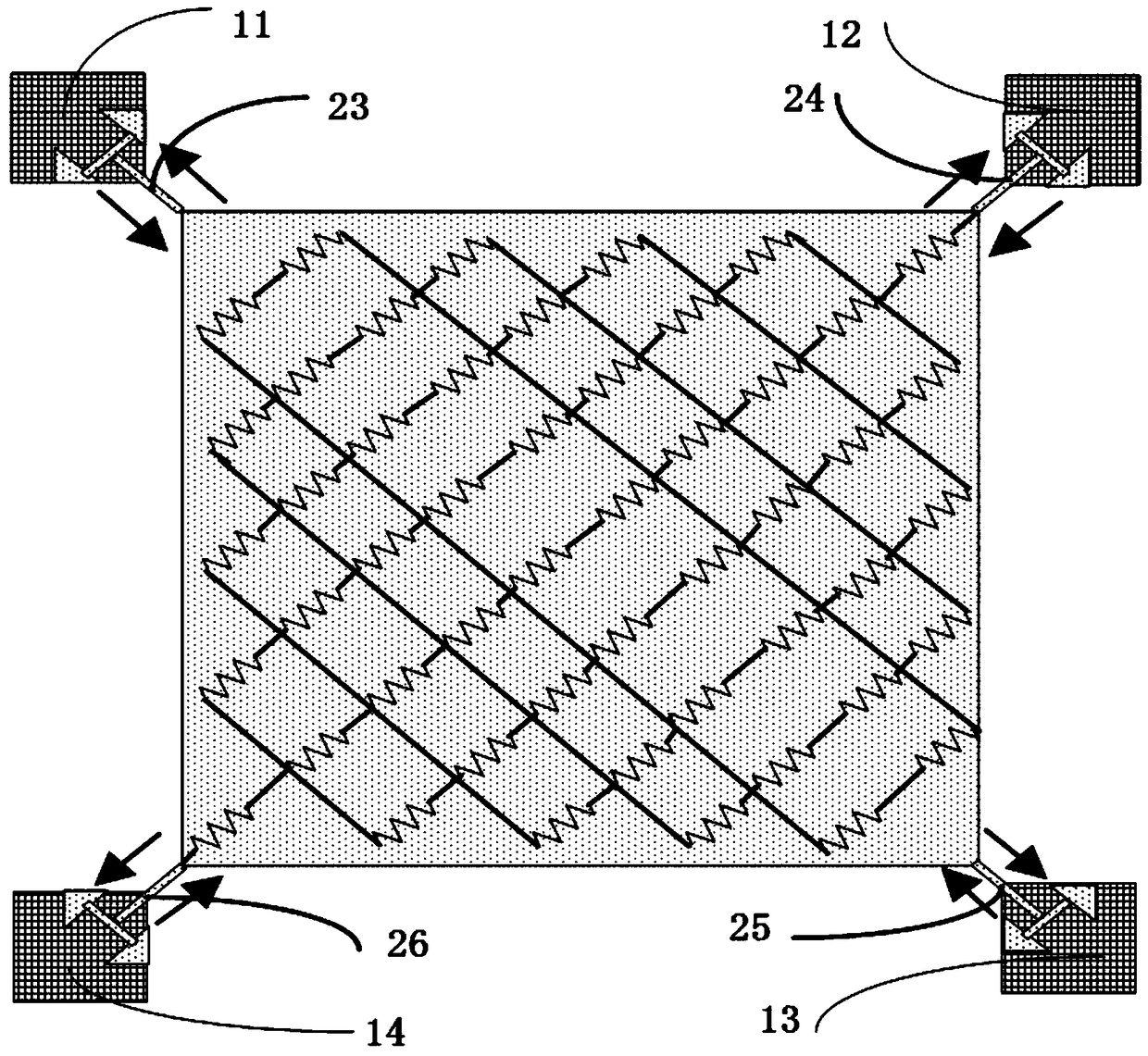
[0031] The present invention will be further described below in conjunction with the accompanying drawings. The following examples are only used to illustrate the technical solution of the present invention more clearly, but not to limit the protection scope of the present invention.

[0032] The two resonant sensor chips are hereinafter referred to as resonator I and resonator II.

[0033] Such as figure 1 As shown, since the monocrystalline silicon material is anisotropic, its piezoresistive coefficient is related to the crystal orientation. In the design of stress-sensitive devices, there are mainly two types of crystal orientations: and crystal planes. When the orientation of the resistance is in the crystal direction, the piezoresistive coefficient is the largest, so in the present invention, the piezoresistive distribution on the surface of the single crystal silicon nano-resonant thin film is along the crystal direction. At this time, the surface of the single cry...


PUM


Abstract

The invention discloses a giant-piezoresistance dual-resonance mass sensor and a making method thereof. The giant-piezoresistance dual-resonance mass sensor comprises sensor chips and an external circuit, and is characterized in that the sensor chips comprise two resonance-type sensor chips connected via a fine nano rod and a temperature compensation device chip; the resonance-type sensor chip comprises a sensitive structure of the resonance-type sensor, a silicon bottom layer, an insulated silicon dioxide layer, a silicon top layer, an aluminum top layer, an excitation electrode, an excitation electrode leading-out end electrode and a detection electrode; the silicon bottom layer, the insulated silicon dioxide layer and the silicon top layer are arranged sequentially from bottom to top; and the aluminum top layer and the silicon top layer are located on the same layer. The surface of a single crystal silicon nano resonance film is processed via a modification process, residual stress is left, and the strain coefficient is about 2 to 3 orders of magnitude higher compared with that of the traditional silicon piezoresistance-type resonance film. In addition, in order to eliminate influences on the piezoresistance value by the temperature, a temperature compensation device is introduced, and the measurement resolution and the measurement sensitivity are greatly improved.

Description

technical field [0001] The invention relates to a giant piezoresistive double-resonant mass sensor and a manufacturing method thereof, belonging to the technical field of micro-nano electro-mechanical systems (MEMS / NEMS). Background technique [0002] In recent years, micro-nano mechanical resonators have been widely developed as high-sensitivity mass sensors. This type of sensor mainly converts the change of the external mass or pressure into the change of the corresponding resonant frequency, and then obtains the relationship between the frequency and the mass or pressure. Get the mass value of the object to be measured. In the field of biochemical sensing, the quartz crystal microbalance (QCM) that has been put into use uses this principle: the change in the surface quality of the quartz crystal oscillator electrode is converted into the frequency change of the output electrical signal of the quartz crystal oscillator circuit, and then through computers and other auxiliar...

Claims


Application Information

Patent Timeline
Patent Type & Authority Patents(China)
IPC IPC(8): G01G3/13B81B7/00B82Y40/00
CPCB81B7/0009B82Y40/00G01G3/13
Inventor 张加宏潘周光葛益娴李敏孙林峰
Owner 南京知行慧芯科技有限公司
Why Eureka
Try Eureka