Miniaturized ultra wide band filter with two-notch features

An ultra-wideband filter and double-notch technology, which is applied in the field of communication, can solve the problems of increasing filter size, high processing technology requirements, and serious reflection loss, etc., and achieve a reduction in overall size, flexible and diverse structural design, and low cost. Effect

Inactive Publication Date: 2016-07-13
CHONGQING UNIV OF POSTS & TELECOMM
View PDF1 Cites 22 Cited by
  • Summary
  • Abstract
  • Description
  • Claims
  • Application Information

AI Technical Summary

Problems solved by technology

[0003] At present, the main design methods to realize the notch characteristics on the ultra-wideband filter include: 1. Loading the open-circuit stub structure, it is necessary to load one or more sections on the original filter whose length is a quarter of the required notch frequency Wavelength open stub line, this method is simple and easy to operate, but the processing technology requirements are high, and the reflection loss is relatively serious; 2. Asymmetric input\output structure, asymmetric input\output coupling line can introduce transmission zero point, and then introduce notch, However, the structure is single, and the control degree of freedom of the notch position is small, so it is not a common design method; 3. The structure of the coupled notch resonator is easier than the previous two methods of introducing notches Controls notch position as well as notch depth, but also increases filter size

Method used


Image

  • Miniaturized ultra wide band filter with two-notch features
  • Miniaturized ultra wide band filter with two-notch features
  • Miniaturized ultra wide band filter with two-notch features

Examples


Embodiment Construction

[0021] Below in conjunction with accompanying drawing, the present invention will be further described:

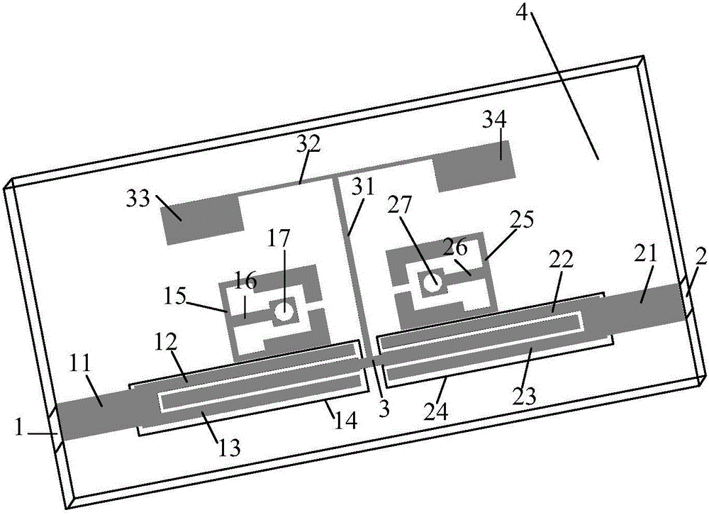
[0022] Such as figure 1 As shown, the UWB filter of the present invention is made up of input / output ports 1 and 2, the upper microstrip structure of the dielectric substrate 4, the dielectric substrate and the bottom metal ground plate of the dielectric substrate, and there are two input / output ports, They are respectively the first input / output port 1 and the second input / output port 2.

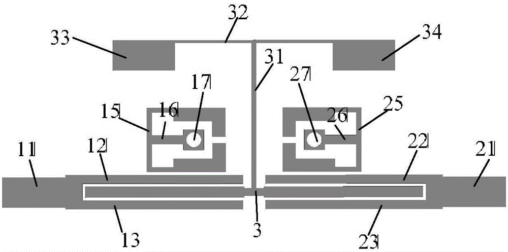
[0023] Such as figure 2 As shown, the upper microstrip structure of the dielectric substrate includes: a first uniform transmission line unit 11, a second uniform transmission line unit 21, a first parallel coupled feeder 12 and 13, a second parallel coupled feeder 22 and 23, a stepped impedance resonator 3, Loaded "T" stubs 31, 32, 33 and 34, first band stop units 15, 16 and 17 and second band stop units 25, 26 and 27; first uniform transmission line unit 11, second uniform transmis...


PUM


Abstract

The invention provides a miniaturized ultra wide band filter with two-notch features, which is composed of two input / output ports, a dielectric substrate, an upper-layer microstrip structure and a bottom metal grounding board of the dielectric substrate, wherein the upper-layer microstrip structure comprises two uniform transmission line units, two first parallel coupled feeder lines, a stepped impedance resonator, a loaded T-type stub and two bandstop units, each bandstop unit comprises an open-loop stepped impedance transmission line and a short circuit stub, and short circuit is realized via a metallized through hole; the bottom metal grounding board comprises a first defect unit, a second defect unit, a first metallized through hole, a second metallized through hole and a grounding metal unit; and the two input / output ports are respectively connected with the upper-layer microstrip structure and the bottom metal grounding board of the dielectric substrate. Through coupling the two bandstop units with the parallel coupled feeder lines respectively, notch features can be realized, and the filter of the invention has the advantages of compact structure, high frequency selectivity and the like.

Description

technical field [0001] The invention belongs to the technical field of communication, in particular to a compact ultra-wideband filter with double notch characteristics and capable of suppressing wireless local area network (WLAN) interference signals and satellite communication interference signals. Background technique [0002] With the rapid development of wireless communication technology, people's demand for information systems continues to increase, and ultra-wideband (UWB) technology has emerged as a new wireless communication technology. In 2002, the U.S. Federal Communications Commission (FCC) officially approved the commercial license of ultra-wideband technology, releasing the communication frequency band from 3.1GHz to 10.6GHz, and ultra-wideband technology was used for civilian use. Compared with other communication technologies, ultra-wideband technology has the advantages of low cost, low power consumption, fast data transmission, and high security, and has be...

Claims


Application Information

Patent Timeline
Patent Type & Authority Applications(China)
IPC IPC(8): H01P1/203
CPCH01P1/20354
Inventor 王斌荆麟尹波张红升黄文
Owner CHONGQING UNIV OF POSTS & TELECOMM
Why Eureka
Try Eureka