Surface polylysine modifying method for PDMS micro-fluidic chip

A microfluidic chip and polylysine technology, applied in the field of microfluidics, can solve the problems of poor sensitivity of the chip substrate, weak dynamic binding, low signal detection value, etc., to achieve the solution of weak binding, The effect of low coefficient of variation between points and high signal-to-noise ratio

Active Publication Date: 2016-07-20
北京乐普诊断科技股份有限公司
View PDF10 Cites 4 Cited by
  • Summary
  • Abstract
  • Description
  • Claims
  • Application Information

AI Technical Summary

Problems solved by technology

However, the sensitivity of poly-lysine-modified chip substrates is not good, and the minimum detection limit is high, especially poly-lysine is physically adsorbed to the chip substrate rather than covalently bound, resulting in dynamic binding to proteins in microfluidic channels. Not firm, low signal detection value

Method used

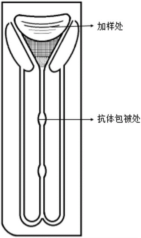

Image

  • Surface polylysine modifying method for PDMS micro-fluidic chip
  • Surface polylysine modifying method for PDMS micro-fluidic chip
  • Surface polylysine modifying method for PDMS micro-fluidic chip

Examples


Embodiment 1

[0038] In this embodiment, the poly-lysine modification on the surface of the PDMS microfluidic chip is carried out by the following method, which specifically includes the following steps:

[0039] (1) The PDMS microfluidic chip is ultrasonically cleaned with deionized water, and then treated with plasma for 10 minutes, the plasma generation power is 10kw, and the plasma air flow rate is 200mL / min to obtain the PDMS microfluidic after plasma activation. control chip;

[0040] (2) Place the PDMS microfluidic chip after the plasma activation treatment in an APTMS solution with a concentration of 1%, and treat it at 65° C. for 60 minutes to obtain a silanized PDMS microfluidic chip, dry it with nitrogen, and wash it with water. Then dry it with nitrogen gas and set aside.

[0041] (3) The silanized PDMS microfluidic chip is placed in a polylysine solution, and covalently bonded under the action of a cross-linking agent. The amount of the cross-linking agent is such that its con...

Embodiment 2

[0043] In this embodiment, the poly-lysine modification on the surface of the PDMS microfluidic chip is carried out by the following method, which specifically includes the following steps:

[0044] (1) The PDMS microfluidic chip is ultrasonically cleaned with deionized water, and then treated with plasma for 3 minutes, the plasma generation power is 20kw, and the plasma air flow rate is 250mL / min to obtain the PDMS microfluidic after plasma activation. control chip;

[0045] (2) Place the PDMS microfluidic chip after the plasma activation treatment in an APTMS solution with a concentration of 2%, and treat it at 60° C. for 45 minutes to obtain a silanized PDMS microfluidic chip, dry it with nitrogen, and wash it with water. Then dry it with nitrogen gas and set aside.

[0046] (3) The silanized PDMS microfluidic chip is placed in a polylysine solution, and covalently bonded under the action of a cross-linking agent. The amount of the cross-linking agent is such that its conc...

Embodiment 3

[0048] In this embodiment, the poly-lysine modification on the surface of the PDMS microfluidic chip is carried out by the following method, which specifically includes the following steps:

[0049] (1) The PDMS microfluidic chip is ultrasonically cleaned with deionized water, and then treated with plasma for 15 minutes, the plasma generation power is 15kw, and the plasma air flow rate is 200mL / min to obtain the PDMS microfluidic after plasma activation. control chip;

[0050] (2) Place the PDMS microfluidic chip after the plasma activation treatment in an APTMS solution with a concentration of 5%, and treat it at 50° C. for 90 minutes to obtain a silanized PDMS microfluidic chip, dry it with nitrogen, and wash it with water. Then dry it with nitrogen gas and set aside.

[0051] (3) The silanized PDMS microfluidic chip is placed in a polylysine solution, and covalently bonded under the action of a cross-linking agent. The amount of the cross-linking agent is such that its con...


PUM


Abstract

The invention provides a surface polylysine modifying method for a PDMS micro-fluidic chip.The PDMS micro-fluidic chip is subjected to plasma processing and silanization processing, and then coupled with polylysine, polylysine is firmly bound to the surface of the chip in a covalent binding mode, and the micro-fluidic chip capable of efficiently fixing protein is formed.According to the modified chip, the common advantages of being high in signal-to-noise ratio, high in binding capacity, low in inter-point variation coefficient and the like of a polylysine modifying method are kept, and more importantly, the problem that polylysine and the chip are bound infirmly in a physical absorption mode, and consequently polylysine is prone to fall off especially in microfluidics application is solved.

Description

technical field [0001] The invention belongs to the technical field of microfluidics, and relates to a method for modifying the surface of a PDMS microfluidic chip with polylysine. Background technique [0002] Microfluidics is a technology that precisely controls and manipulates microscale fluids, especially submicron structures. The microfluidic chip integrates sample preparation, reaction, separation, detection and other operations on a one-micron chip, and automatically completes the analysis. It has the characteristics of less required samples, small size, easy to carry, fast detection speed, and high-throughput screening. Fluidics has developed rapidly in the fields of biology, medicine, chemistry, materials, and electronics. [0003] The most important procedure in the preparation of microfluidic chips is the immobilization of proteins on the substrate. Whether proteins can be efficiently and firmly immobilized on the substrate carrier and maintain good biological ac...

Claims


Application Information

Patent Timeline
Patent Type & Authority Applications(China)
IPC IPC(8): B01L3/00
CPCB01L3/502707B01L2200/12B01L2300/12B01L2300/16
Inventor 张单单胡飞熊晶邱笑违余占江
Owner 北京乐普诊断科技股份有限公司
Why Eureka
Try Eureka