High boost multiple charge pump circuit for mems switch and manufacturing method thereof

A charge pump and circuit technology, which is applied in the direction of circuits, semiconductor/solid-state device manufacturing, electrical components, etc., can solve problems such as circuit high-voltage breakdown, achieve high withstand voltage, low power consumption, and reduce losses

Active Publication Date: 2019-07-12
NO 55 INST CHINA ELECTRONIC SCI & TECHNOLOGYGROUP CO LTD
View PDF5 Cites 0 Cited by
  • Summary
  • Abstract
  • Description
  • Claims
  • Application Information

AI Technical Summary

Problems solved by technology

On the other hand, as the boost multiple increases, high voltage breakdown in the circuit will also become a problem. These are the problems faced by the design of high boost multiple charge pump circuits.

Method used


Image

  • High boost multiple charge pump circuit for mems switch and manufacturing method thereof
  • High boost multiple charge pump circuit for mems switch and manufacturing method thereof
  • High boost multiple charge pump circuit for mems switch and manufacturing method thereof

Examples


Embodiment 1

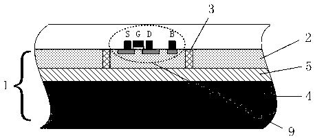
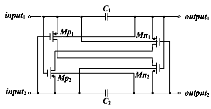
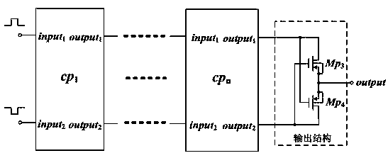
[0038] High boost multiple charge pump circuit for MEMS switches: its structure includes: SOI wafer 1, top layer silicon 2, Trench structure 3, high-resistance carrier 4, silicon dioxide layer 5, layout of the first Trench structure 6, second Trench Layout 7 of the structure, layout 8 of the third Trench structure, MOS tube 9, and MOS tube capacitor; wherein, the SOI wafer 1 is divided into the top layer silicon 2, the silicon dioxide layer 5, the high resistance carrier 4, and the SOI wafer 1 from top to bottom. Trench structure 3 is performed on the top layer of silicon 2 of wafer 1 to realize the electrical isolation of each MOS transistor 9 substrate. MOS transistor 9 and MOS transistor capacitor interconnection form a charge pump sub-circuit, and several stages of charge pump sub-circuits and output stages are cascaded to form a the entire charge pump circuit.

[0039] The overall layout of the charge pump circuit adopts a symmetrical structure up and down, the layout 6 o...


PUM


Abstract

The present invention is a high boost multiple charge pump circuit for a MEMS switch. Its structure is that the layout of the second Trench structure and the layout of the third Trench structure respectively surround the layout of the first Trench structure. The SOI wafer is top-layer silicon from top to bottom. Silicon oxide layer, high-resistance carrier; Trench structure is carried out on the top silicon of the SOI wafer to realize electrical isolation of each MOS transistor substrate, and the interconnection between the MOS transistor and the third capacitor constitutes a charge pump sub-circuit unit, and several stages of charge pump sub-circuits The circuit unit and the output stage are cascaded to form the whole charge pump circuit. The invention has the advantages that all the circuits adopt CMOS technology, and have the advantages of high integration, low power consumption, easy to obtain high boosting multiple, and the like.

Description

technical field [0001] The invention relates to a high boost multiple charge pump circuit for MEMS switches and a manufacturing method thereof, belonging to the technical field of semiconductor integrated circuits. Background technique [0002] RF_MEMS switches have become the key components to improve the performance of radio frequency systems due to their advantages such as high linearity, high bandwidth, high isolation, and low power consumption. Its driving also has the characteristics of high voltage and low current, especially in the case of high reliability contact, the driving voltage is required to reach 30~90V, and the current is below the nanoampere level. However, increasingly miniaturized radio frequency systems, especially hand-held micro-systems, have a power supply voltage of only a few volts, which cannot directly provide a high enough driving voltage to make MEMS switches work reliably. Therefore, a boost circuit chip with a high boost multiple is needed t...

Claims


Application Information

Patent Timeline
Patent Type & Authority Patents(China)
IPC IPC(8): H01L21/762H01L27/12H02M3/07
CPCH01L21/76264H01L21/76283H01L27/1203H02M3/07H02M1/007
Inventor 孙俊峰朱健郁元卫李晓鹏
Owner NO 55 INST CHINA ELECTRONIC SCI & TECHNOLOGYGROUP CO LTD
Why Eureka
Try Eureka