Aluminum-gallium-nitride compound/gallium nitride high-electron mobility transistor

A high electron mobility, compound technology, applied in transistors, circuits, electrical components, etc., can solve the problems of 2DEG concentration reduction, redistribution, device performance consistency and adverse effects on reliability, etc. Effects of redistribution, improved consistency and reliability

Active Publication Date: 2016-07-20
NO 55 INST CHINA ELECTRONIC SCI & TECHNOLOGYGROUP CO LTD
View PDF4 Cites 8 Cited by
  • Summary
  • Abstract
  • Description
  • Claims
  • Application Information

AI Technical Summary

Problems solved by technology

Another use of the introduction of the GaN cap layer is to curb the current collapse of AlGaN / GaNHEMT (R.Coffieetal., IEEE ElectronDeviceLett., Vol.23, No.10, pp.588-590, 2002.), but its disadvantage is It will cause the decrease of 2DEG concentration in the channel. In addition, the source electrode and drain electrode of conventional AlGaN / GaN HEMT devices are directly deposited on the GaN cap layer, and need to form ohmic contact with the epitaxial layer under the superalloy process. During the high temperature process, the source electrode and the drain electrode The drain electrode metal needs to penetrate the GaN cap layer, AlGaN barrier layer and AlN insertion layer to form ohmic contact with the 2DEG in the channel. Generally speaking, when there are GaN cap layer and AlN insertion layer, to obtain better ohmic contact, you need Using a higher alloy temperature will make the thermal expansion and contraction of the source electrode and drain electrode metal more serious during the alloying process, and even lead to the redistribution of epitaxial layer stress, which is detrimental to the consistency and reliability of device performance influences

Method used


Image

  • Aluminum-gallium-nitride compound/gallium nitride high-electron mobility transistor
  • Aluminum-gallium-nitride compound/gallium nitride high-electron mobility transistor
  • Aluminum-gallium-nitride compound/gallium nitride high-electron mobility transistor

Examples


Embodiment Construction

[0011] Below in conjunction with accompanying drawing, the present invention is further described in detail:

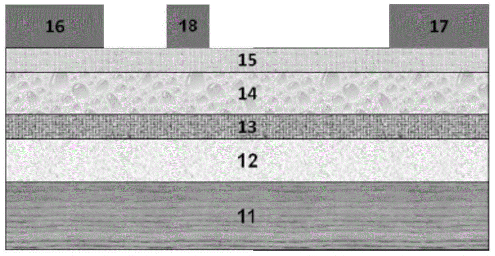
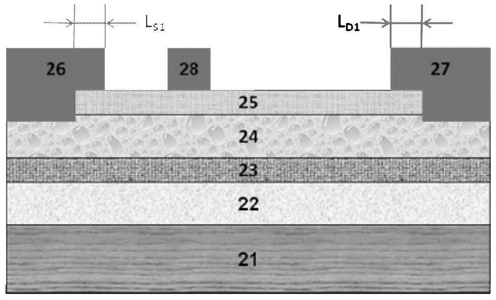
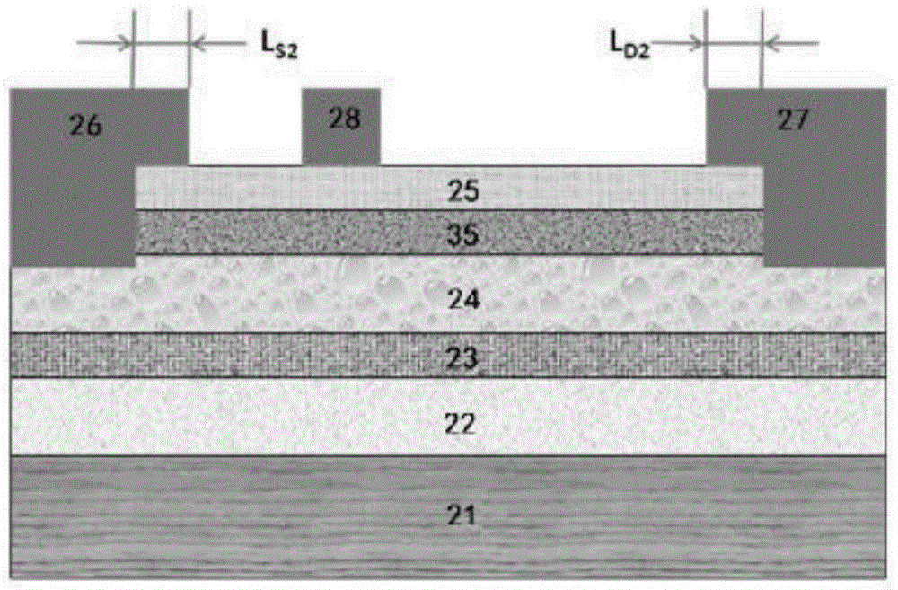
[0012] figure 2 Shown is an embodiment of the AlGaN / GaN HEMT according to the present invention. The AlGaN / GaN HEMT according to the present invention has a substrate 21, the substrate 21 is any one of sapphire, Si and SiC, preferably semi-insulating 4H- SiC and semi-insulating 6H-SiC are used as substrates, and semi-insulating 4H-SiC (0001) and semi-insulating 6H-SiC (0001) are used as substrates, which have high thermal conductivity and small lattice mismatch with GaN It is not only easy to grow high-quality GaN epitaxial materials, but also conducive to the heat dissipation of devices. Currently, Cree and II-VI companies in the United States sell SiC substrates in both 4H and 6H forms.

[0013] The GaN buffer layer 22 is located on the substrate 21, and the thickness of the GaN buffer layer is preferably 1500-2000nm. The GaN buffer layer 22 generally has a higher...


PUM


Abstract

The invention discloses a nitride high-mobility transistor with aluminum-gallium-nitride compound insertion layers for a strain balance. The nitride high-mobility transistor comprises a substrate, a GaN buffer layer, an Al<y>Ga<1-y>N insertion layer, an Al<x>Ga<1-x>N barrier layer and a GaN cap layer, wherein the GaN buffer layer is located on the substrate; the Al<y>Ga<1-y>N insertion layer is located on the GaN buffer layer; the Al<x>Ga<1-x>N barrier layer is opposite to the GaN buffer layer and is located on the Al<y>Ga<1-y>N insertion layer; the GaN cap layer is located on the Al<x>Ga<1-x>N barrier layer; the GaN cap layer and partial thickness of the Al<x>Ga<1-x>N barrier layer are removed to form grooves; inverted L-shaped source electrode and drain electrode are provided in the grooves respectively; and a gate electrode is located between the source electrode and the drain electrode. According to the other embodiment of the invention, an Al<z>Ga<1-z>N insertion layer is also formed between the Al<x>Ga<1-x>N barrier layer and the GaN cap layer. The aluminum-gallium-nitride compound / gallium nitride high-electron mobility transistor has the advantages that the performance of the AlN insertion layer is achieved by high-Al component AlGaN insertion layers; the processing controllability is relatively high; formation of an ohmic contact is facilitated by introduced inverted L-shaped source electrode and drain electrode; and meanwhile, the overall stress of an epitaxial layer can be relatively well controlled by combining the GaN cap layer, so that the performance is optimized when the reliability of the device is ensured.

Description

technical field [0001] The invention relates to a nitride high-mobility transistor with AlGaN intercalation layer strain balance. Background technique [0002] Aluminum Gallium Nitride (AlGaN) / Gallium Nitride (GaN) High Electron Mobility Transistor (HEMT), as the third-generation wide bandgap compound semiconductor device, has the characteristics of high output power, high operating frequency, high temperature resistance, etc., especially its combined Some high-frequency and high-power characteristics are not available in existing semiconductor technologies such as Si and GaAs, which makes it have a unique advantage in leading microwave applications, thus becoming a hot spot in the research of semiconductor microwave power devices. Through the introduction of AlN insertion layer (L.Shenetal., IEEE Electron Device Lett., vol.22, pp.457–459, Oct.2001.) combined with the improvement of the crystal quality of epitaxial materials, the introduction of SiN surface passivation techn...

Claims


Application Information

Patent Timeline
Patent Type & Authority Applications(China)
IPC IPC(8): H01L29/778H01L29/06H01L29/08
CPCH01L29/06H01L29/0843H01L29/401H01L29/778H01L21/02378H01L21/02433H01L21/02458H01L21/02505H01L21/0254H01L21/28575H01L21/28587H01L29/2003H01L29/205H01L29/207H01L29/41766H01L29/475H01L29/7786H01L21/02579H01L21/02598H01L21/0262H01L21/02631H01L21/246H01L21/30621H01L29/1029H01L29/41775H01L29/454H01L29/66462H01L29/66863
Inventor 任春江陈堂胜
Owner NO 55 INST CHINA ELECTRONIC SCI & TECHNOLOGYGROUP CO LTD
Why Eureka
Try Eureka