Formation method of transistor

A transistor and substrate technology, applied in semiconductor devices, semiconductor/solid-state device manufacturing, electrical components, etc., can solve problems affecting the performance of semiconductor devices, defects in semiconductor devices, etc., to achieve the effect of optimizing performance and reducing the number of traps

Active Publication Date: 2016-08-03
SEMICON MFG INT (SHANGHAI) CORP
View PDF6 Cites 5 Cited by
  • Summary
  • Abstract
  • Description
  • Claims
  • Application Information

AI Technical Summary

Problems solved by technology

[0006] However, when a hafnium-based high-K material is used as a gate dielectric material, it is easy to generate defects in the semiconductor device and affect the performance of the semiconductor device.

Method used


Image

  • Formation method of transistor
  • Formation method of transistor
  • Formation method of transistor

Examples


Embodiment Construction

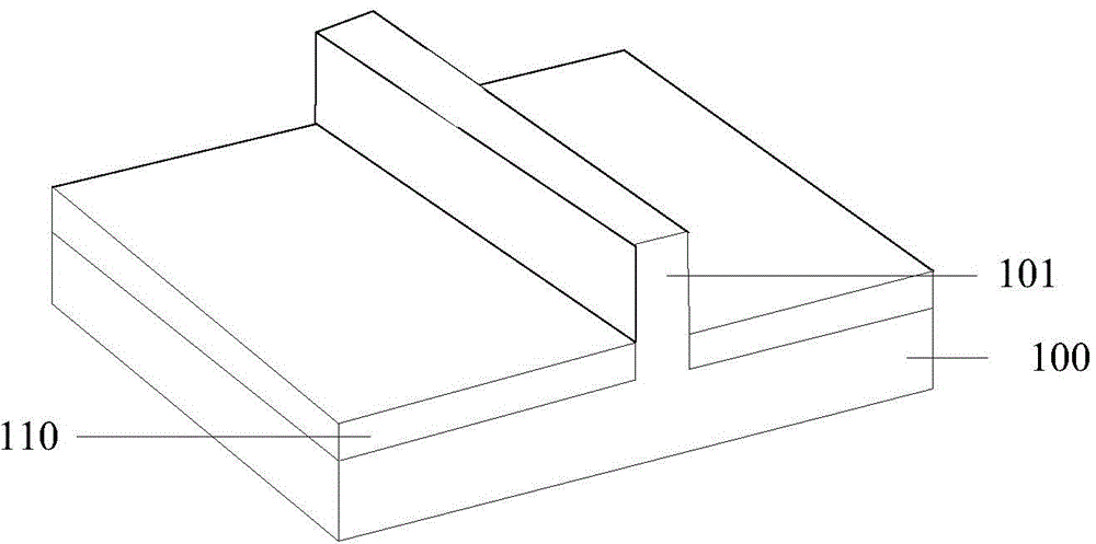
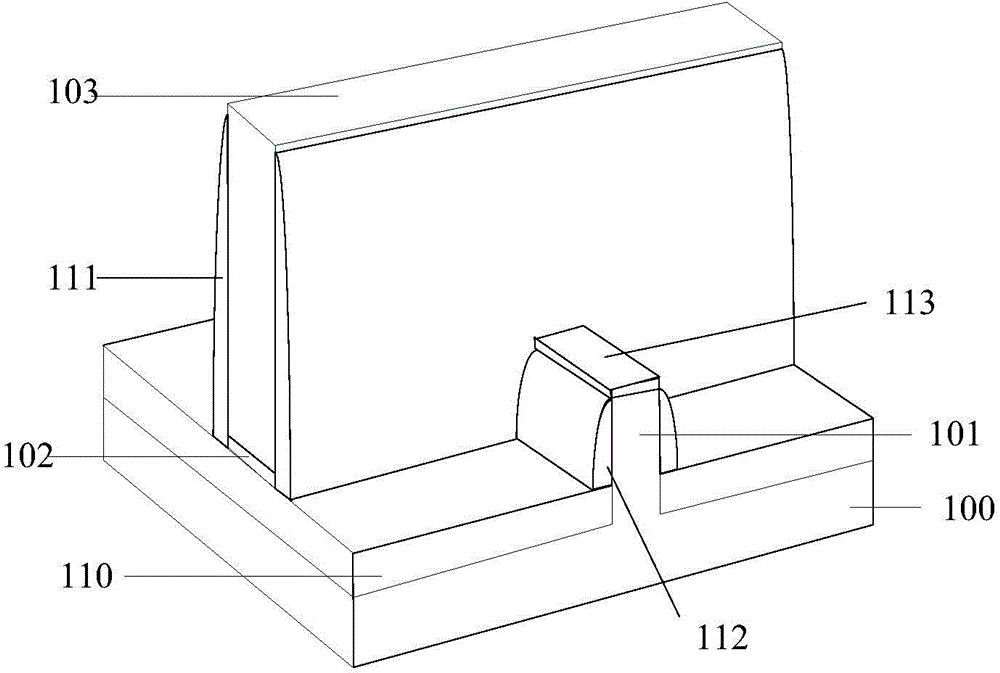
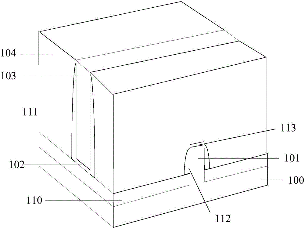
[0035] In the prior art, when the hafnium-based high-K material is used as the material of the gate dielectric layer, it is easy to generate defects in the semiconductor device, thereby affecting the performance of the semiconductor device. Analyzing the causes of defects in semiconductor devices, trap defects are prone to occur in hafnium-based high-K materials, and interface state defects are also prone to occur at the interface between hafnium-based high-K materials and silicon substrates. A silicon oxide layer is added between the high-K material and the silicon substrate to reduce interface state defects, but in actual production, problems such as increased leakage current and threshold voltage drift caused by interface state defects are still serious.

[0036] For this reason, the present invention provides a method for forming a transistor. In the method for forming a transistor of the present invention, a hafnium-based dielectric layer is formed at the bottom of the ope...


PUM


Abstract

The invention provides a formation method of a transistor, which comprises the steps of providing a transistor, forming a pseudo gate structure on the substrate, forming a source region and a drain region in the substrate at two sides of the pseudo gate structure, forming an interlayer dielectric layer, which is flush with the pseudo gate structure, on the substrate, removing the pseudo gate structure and forming an opening from which part of the substrate is exposed, forming a hafnium-based high-dielectric layer at the bottom of the opening so as to act as a gate dielectric layer, carrying out first annealing, wherein an oxygen-containing gas is charged in the process of the first annealing, and carrying out second annealing, wherein hydrogen is charged in the process of the second annealing. In the first annealing, oxygen ions supplement oxygen vacancies in the hafnium-based high-dielectric layer, and the number of traps caused by the oxygen vacancies is reduced; and in the second annealing, hydrogen ions supplement an interface between the gate dielectric layer and the substrate, and the number of traps caused by an interface state defect is reduced, thereby being capable of optimizing the performance of the transistor.

Description

technical field [0001] The invention relates to the field of semiconductor manufacturing, in particular to a method for forming a transistor. Background technique [0002] With the rapid development of integrated circuit (abbreviated as IC) manufacturing technology, the size of semiconductor devices is constantly shrinking, which affects the performance of semiconductor devices. [0003] For example: channel length and gate dielectric layer (usually SiO2) in MOS transistors 2 ) thickness is scaled down, resulting in defects such as polysilicon loss, higher gate resistance, and increased leakage current. For this reason some high K (dielectric constant) dielectric materials replace traditional SiO 2 It can effectively reduce gate leakage current, but high-K dielectric materials are not compatible with polysilicon, so most current integrated circuits use metal gate electrodes instead of polysilicon gate electrodes, and achieve good results. [0004] The equivalent oxide thi...

Claims


Application Information

Patent Timeline
Patent Type & Authority Applications(China)
IPC IPC(8): H01L21/28H01L21/336
Inventor 周飞居建华
Owner SEMICON MFG INT (SHANGHAI) CORP
Why Eureka
Try Eureka