Formation method of semiconductor structure

A semiconductor and graphics layer technology, applied in the field of semiconductor structure formation, can solve the problems of semiconductor structure yield chip output, conduction performance, and contact resistance reduction, and achieves easy control of feature size and improved chip performance. Yield, uniformity improvement effect

Active Publication Date: 2019-12-03
SEMICON MFG INT (SHANGHAI) CORP
View PDF4 Cites 0 Cited by
  • Summary
  • Abstract
  • Description
  • Claims
  • Application Information

AI Technical Summary

Problems solved by technology

However, the conduction performance between the metal plug and the gate structure, the source region and the drain region needs to be improved and the contact resistance is relatively large. In order to improve the contact resistance between the metal plug and the gate structure, the source region and the drain region, usually Form metal silicide (Silicide), such as nickel silicide, on the surface of the source region, drain region and gate structure to reduce the contact resistance between the metal plug and the gate structure, source region and drain region
[0004] However, the yield rate and chip output of the prior art semiconductor structures still need to be improved

Method used


Image

  • Formation method of semiconductor structure
  • Formation method of semiconductor structure
  • Formation method of semiconductor structure

Examples


Embodiment Construction

[0032] It can be seen from the background art that the yield rate of the semiconductor structure formed in the prior art needs to be improved, and the output of chips is low.

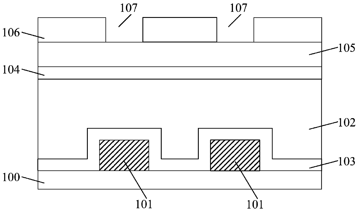
[0033]In one embodiment, the formation process of the semiconductor structure includes the following steps: step S1, providing a substrate, the substrate has an underlying metal layer, and forming a dielectric layer on the surface of the substrate; step S2, forming a pattern on the surface of the dielectric layer layer, the graphic layer has an opening exposing the surface of the dielectric layer; step S3, using the graphic layer as a mask, etching the dielectric layer along the opening until the surface of the underlying metal layer is exposed, and forming a contact in the dielectric layer hole; step S4, performing wet cleaning on the contact hole; step S5, forming a conductive layer filling the contact hole.

[0034] In the above methods, the dielectric layer is generally etched by a dry etching proce...


PUM

PropertyMeasurementUnit
contact angleaaaaaaaaaa
relative permittivityaaaaaaaaaa

Abstract

The invention provides a method for forming a semiconductor structure. The method comprises a step of providing a substrate with a bottom metal layer, a step of forming a dielectric layer which covers the surface of the substrate and the surface of the bottom metal layer, a step of forming a pattern layer at the surface of the dielectric layer, wherein the pattern layer has an opening inside, a step of etching the dielectric layer along the opening with the pattern layer as a mask until the surface of the bottom layer is exposed, forming a contact hole with a fluorine-containing polymer impurity in the dielectric layer, a step of removing the pattern layer, a step of using a hydrogen plasma to carry out first etching processing on the contact hole, and removing the fluoride ion in the fluorine-containing polymer impurity, a step of carrying out wet cleaning processing on the contact hole after the first etching processing, and a step of forming a conductive layer which fills the contact hole. According to the method, the damage of the dielectric layer and the bottom layer metal layer by the fluorine ion in Q-time is avoided, the production yield of the semiconductor structure is improved, and the chip output amount is raised.

Description

technical field [0001] The invention relates to the technology in the field of semiconductor manufacturing, in particular to a method for forming a semiconductor structure. Background technique [0002] With the development of integrated circuits to ultra-large scale integrated circuits, the circuit density inside integrated circuits is increasing, and the number of components contained is also increasing. In a semiconductor integrated circuit, a Metal Oxide Semiconductor (MOS, Metal Oxide Semiconductor) transistor is one of the most important components. [0003] The existing MOS transistor process is to form a gate structure on a semiconductor substrate, and form a source region and a drain region in the semiconductor substrate on opposite sides of the gate structure; then form contacts on the gate structure, source region and drain region Hole (Contactvia), the contact hole is filled with metal to form a metal plug. However, the conduction performance between the metal ...

Claims


Application Information

Patent Timeline
Patent Type & Authority Patents(China)
IPC IPC(8): H01L21/768
Inventor 张海洋黄敬勇
Owner SEMICON MFG INT (SHANGHAI) CORP
Why Eureka
Try Eureka